Every leading-edge logic chip made since 2007 switches through a film that was deposited one atomic layer at a time. That film is hafnium oxide, HfO2, and the process is atomic layer deposition, ALD. Silicon dioxide had served as the gate dielectric for four decades; by the mid-2000s it was so thin that electrons tunneled straight through it, and the industry’s answer was a thicker film with a higher dielectric constant, grown with atomic precision.
What the gate dielectric does, and why SiO2 ran out of road
A transistor’s gate sits above the channel, separated by a dielectric. The gate voltage reaches through that dielectric and turns the channel on or off. The thinner the dielectric, the more control the gate has, so for decades the industry thinned SiO2 relentlessly, down to about 1.2 nanometers of equivalent thickness by the mid-2000s. Intel’s own materials explain the numbers: silicon dioxide has a dielectric constant k of 3.9, and at that thickness electrons leak straight through the film by quantum tunneling, wasting power whether the transistor is on or off.
The fix is to swap the material, not fight the physics. A high-k dielectric can be physically thicker while electrically behaving like a much thinner oxide, because capacitance scales with k divided by thickness. HfO2’s dielectric constant is roughly 25, six times better than SiO2, as Real World Tech’s analysis notes, so a film several atoms thicker delivers the same gate control with exponentially less leakage. Intel put HfO2 into production at the 45 nm node in 2007 with metal gates replacing polysilicon, and its press materials credited hafnium with replacing the silicon dioxide gate dielectric outright. EE Times’ contemporaneous reporting confirmed the stack: HfO2 as the dielectric, with titanium nitride-based metal gates tuned separately for NMOS and PMOS.
Why the film had to be ALD
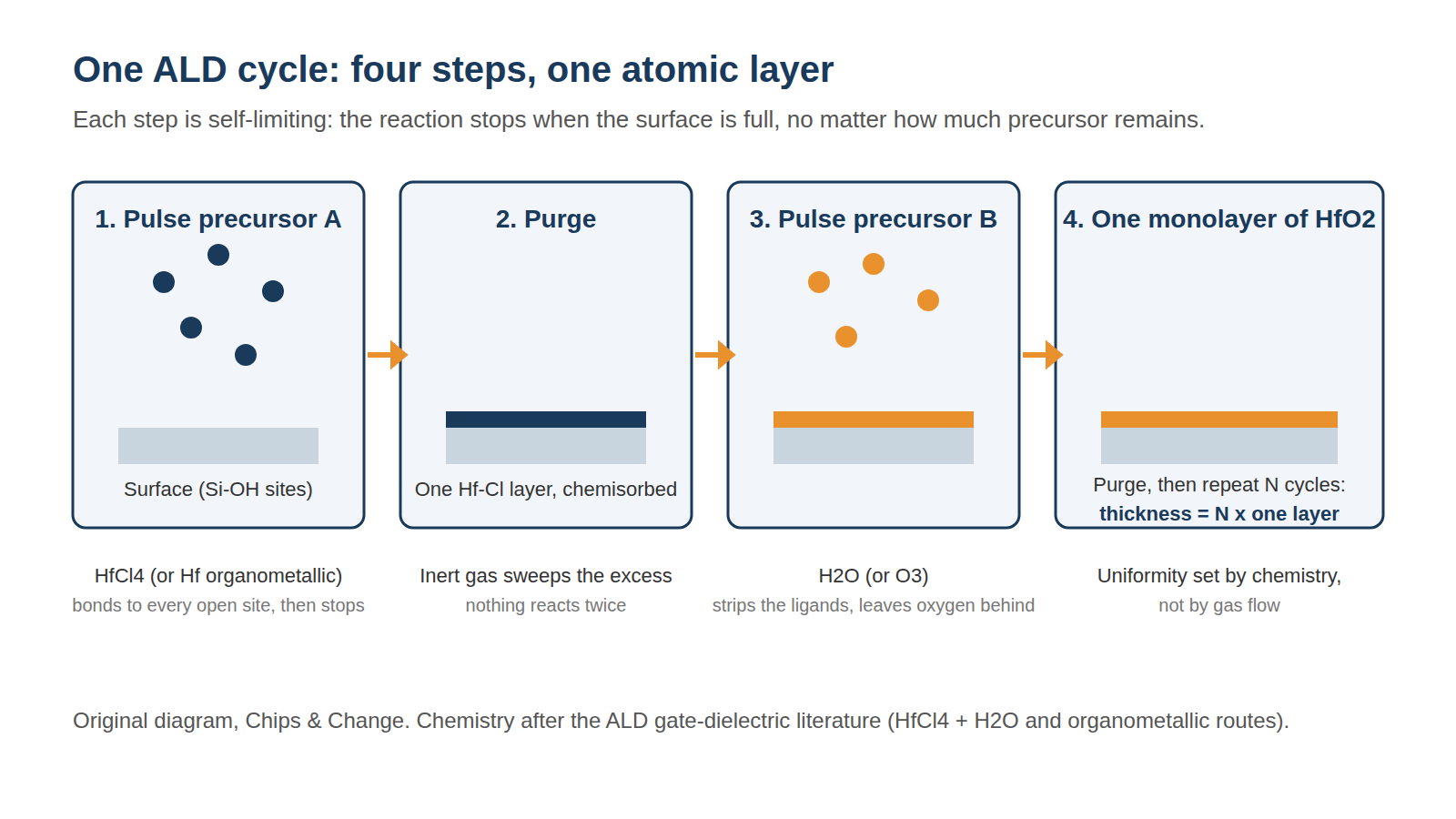
Depositing that film is where ALD earns its place in every fab. In ALD the wafer is exposed to two chemicals in sequence, separated by purge steps. The first bonds to the surface and then stops: once every available site has reacted, the reaction quits on its own, no matter how much more chemical arrives. The second reacts with that layer, again until it self-terminates. One cycle leaves a single atomic layer, and thickness is set by counting cycles, not by tuning gas flows.
That self-limiting behavior is the whole point. In chemical vapor deposition, the film grows as long as precursor keeps arriving, so thickness depends on temperature, flow, and residence time, and it drifts across a wafer. A gate dielectric that varies by half a nanometer across a wafer is broken, because the thinnest spot sets the leakage for the whole chip. Real World Tech’s analysis of Intel’s 45 nm process states it directly: the hafnium gate oxide was deposited using ALD to ensure the gate was uniformly thick. ALD also coats high-aspect-ratio structures conformally, which matters enormously now that gates wrap all around nanosheet channels.
The price is throughput. ALD lays down one layer per cycle, with each cycle taking seconds, so a film that CVD would flash down in one pass takes minutes. Fabs live with it because nothing else delivers the thickness control, and toolmakers have spent two decades raising wafer throughput with multi-chamber platforms. A review in Applied Sciences catalogs the precursor chemistry that made it work: hafnium chloride and water, or organometallic hafnium precursors, with titanium nitride gates from titanium tetrachloride and ammonia.
The subtleties that never made the press release
HfO2 is not a drop-in replacement for SiO2, and the difficulties took years longer to solve than the industry expected. HfO2 reacts with silicon and with gate metals at processing temperatures, and oxygen vacancies in the film trap charge and shift the transistor’s threshold voltage over time. The working solution keeps a thin silicon dioxide interface layer between the HfO2 and the channel, so the film stack is really a sandwich: SiO2 for the interface quality, HfO2 for the capacitance, and metal gates chosen for their work function. Cambridge University’s review of high-k and metal gate research describes how those reactions forced the industry toward gate-last integration, where the replacement metal gate is deposited after the transistor is otherwise finished, to keep the metals from reacting with the dielectric at high temperature.
The same film is now the front-runner for a new memory class. Doped hafnium oxide, typically HfO2 alloyed with zirconium into HZO, is ferroelectric: its crystal structure holds an electric polarization that survives the power coming off, which makes a memory element out of a material fabs already know how to deposit. A 2025 review in Nano Convergence notes that HfO2 was already widely adopted in CMOS through ALD, and that compatibility is what sparked the race toward ferroelectric FeFET and FeCAP memories. Mark Lapedus’ February 2026 survey of ferroelectric development found FeCAPs, FeFETs and FeRAMs all in various stages of development, each combining ferroelectric and doped HfO2 somewhere in the device. The material won its first job in 2007 and is auditioning for its second.
The fab floor read
The lesson of HfO2 is that the industry’s hardest material transitions are won by deposition control, not by discovery. Hafnium oxide was a known insulator for decades; what made it a product was a process that could put down four atomic layers of it, identically, on ten thousand wafers a day. That is why ALD spread from the gate stack to everywhere films must be thin and conformal: DRAM capacitor dielectrics, spacer liners, diffusion barriers, and advanced packaging. It runs a self-limiting reaction, counts its cycles, and never gets a keynote.
FAQ
What does ALD stand for? Atomic layer deposition: a process that deposits one atomic layer per cycle using self-limiting chemical reactions, so thickness is set by the number of cycles.
Why did silicon dioxide stop working as a gate dielectric? Below roughly 1.2 nanometers of equivalent thickness, electrons tunnel directly through SiO2, so leakage current grows even when the transistor is off. A higher-k material such as HfO2 gives the same gate control with a physically thicker film and far less leakage.
When did chips start using HfO2? Intel put HfO2 gate dielectrics with metal gates into production at the 45 nm node in 2007, and every leading-edge logic technology since has used a high-k gate dielectric.
Is HfO2 still used today? Yes, in every leading-edge gate stack, and increasingly as a memory material: zirconium-doped HfO2 is ferroelectric and under development for FeFET and FeCAP memories built with standard fab equipment.