Fab Floor Friday — the week of November 16–20, 2026, from the fab floor up: what changed at the film level, what it costs, and who it helps.
The export-control rule reached the wafer-start meeting
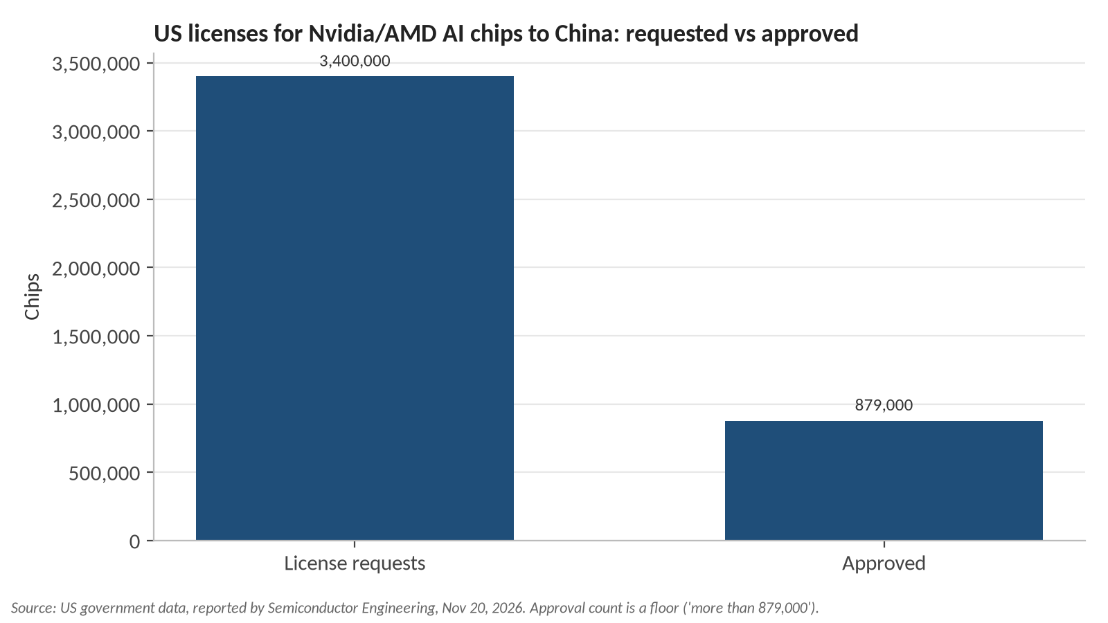
What happened: On November 16 the Commerce Department published an interim final rule restricting remote access to advanced US AI computing from overseas data centers and adding licensing requirements touching Singapore, Malaysia, Thailand, Indonesia, and Brazil, as the Semiconductor Industry Association noted in its statement on the rule. By midweek the Financial Times reported, relayed in Semiconductor Engineering’s week in review, that TSMC and Samsung had suspended some chip shipments to Chinese customers pending licensing approvals, and that TSMC is halting affected Chinese orders at 16nm and below without US approval while generally limiting those customers to 28nm and 40nm processes, provided the chips use no HBM or advanced packaging. TSMC said on Friday it will comply with the rules, which also close the third-country-intermediary route Chinese designers had used to get advanced chips made at overseas foundries. US government data reported in the same week-in-review shows license requests covering 3.4 million advanced Nvidia and AMD AI chips for China, with more than 879,000 approved.
The fab floor read: Export-control stories usually stay in Washington; this one walked into the wafer-start meeting. A foundry qualifies customers and schedules starts weeks ahead, so a license question landing mid-quarter turns qualified lots into lots that cannot ship. The 28/40nm carve-out keeps mature-node revenue flowing, which is why the pain concentrates on designers who already taped out at 16nm and below. This is the operational sequel to Thursday’s post on export controls and the tool ban: the tools were restricted first, and now the wafers the remaining tools can make are being metered too.
Intel signed its first outside customer for 18A-P
What happened: Intel executives said this week that Intel Foundry has signed its first external customer for its 18A-P process; the customer is unnamed and no production timetable was disclosed. Separately, Microsoft selected Intel Foundry’s EMIB advanced packaging for custom silicon used in Azure infrastructure, under a multiyear agreement that also expands cooperation on Xeon processors, memory, and security technologies.
The fab floor read: A signed customer is a design win, not a ramp, and it is worth saying so plainly. But the pair of announcements matters more than either alone: EMIB packaging is where a foundry proves it can handle someone else’s die before it proves it can print them, so buying both says the customer is treating Intel Foundry as a system rather than a lithography roadmap. 18A-P’s distinguishing moves — gate-all-around RibbonFET transistors and backside power delivery — move the hard problems from the front of the wafer to the back, and the read from the floor is that Intel now has outside revenue attached to proving it at scale.
The packaging race went vertical
What happened: Nvidia expanded manufacturing agreements with Amkor, Samsung Electro-Mechanics, SPIL, TSMC, and others covering substrate manufacturing, advanced packaging, and wafer capacity; SPIL, ASE’s subsidiary, signed a multibillion-dollar agreement to triple its advanced packaging capacity in Taiwan by mid-2029. ASE inaugurated the first phase and began construction of the second phase of its Lujhu facility in Kaohsiung. Micron moved the first equipment into its HBM advanced-packaging facility in Singapore, targeting initial production in early 2027, and Kulicke & Soffa shipped its first fluxless thermocompression bonding systems for panel-level packaging to two customers in Taiwan.
The fab floor read: Three announcements, one message: the constraint on AI chip supply this cycle is not wafer output but how fast dies get stacked, bonded, and tested. Fluxless thermocompression bonding is the tell — flux residue is a yield killer at fine-pitch AI-package dimensions, so toolmakers are engineering the contamination out rather than washing it off. Capacity committed now ships in 2027–2029, the same window as HBM4 and co-packaged optics, so the queue is the forecast.
Nvidia wrote China to zero, and the market repriced the week
What happened: Nvidia reported Q3 revenue up 103% year over year, and interim CEO Colette Kress said on the earnings call that the company has stopped shipping licensed Hopper AI chips to China, with the Q4 outlook assuming no data-center compute revenue from China; Nvidia also established an oversight committee for national-security policy and export-control compliance. On Friday, US stocks closed sharply lower, with the S&P 500 and Dow ending in correction, Nvidia down 14.01% on the day and the Nasdaq 100 down 5.67%, according to Stock Titan’s market wrap.
The fab floor read: The durable fact is not Friday’s move but the revenue line: a company that grew 103% while writing its China business to zero has repriced what “global” means in global semiconductor demand. The oversight committee is the org-chart version of the same thing — export-control compliance is now a permanent operating condition, not a news cycle. For equipment and materials suppliers, planning against a market that can be switched off by rulemaking is the new baseline.
That’s the week from the floor. Next Friday, same time.