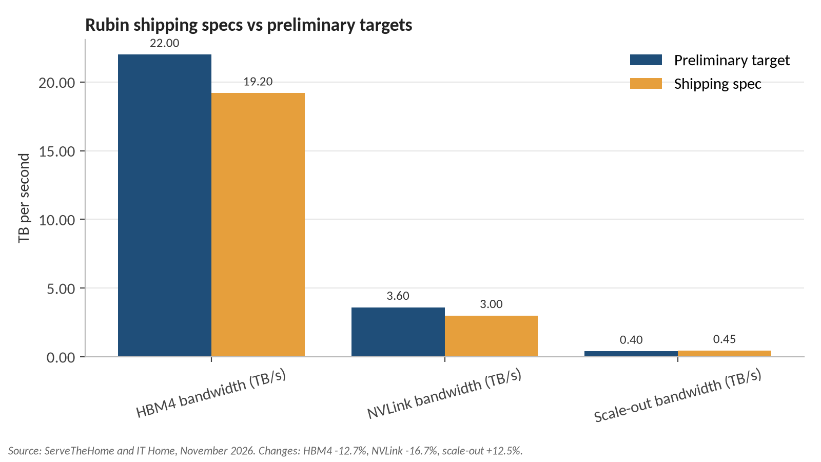
NVIDIA’s Rubin generation is shipping in volume, and the silicon that arrived is not quite the silicon that was promised. The company quietly revised the shipping specifications this fall: HBM4 memory bandwidth came down from 22 to 19.2 TB per second, a cut of about 13 percent per GPU, NVLink scale-up bandwidth dropped 17 percent, and scale-out networking bandwidth went up. Compute targets held. The gap between the brochure and the box is where the real fab-floor story of 2026 lives, because it says the ceiling on AI chips is no longer set by lithography or by transistor density. It is set by packaging and memory.
NVIDIA Rubin specs: what changed and why
Rubin entered full production during 2026 and reached deployment in the fall, with hyperscalers making the first Vera Rubin NVL72 racks generally available. In its first MLPerf Inference v6.1 submission, NVIDIA reported that a Vera Rubin NVL72 rack delivered up to 3.7 times the throughput of the previous GB300 NVL72, and MLCommons published the round with a participation record of 30 submitting organizations and 486 results. A recomputation published by GPU Insights puts the per-accelerator gain at 1.97 times in server and 2.57 times in interactive workloads, which is still a large step and a useful reminder that rack-level marketing numbers and per-chip reality are different quantities.
Then came the specification revisions, spotted by IT Home and detailed by ServeTheHome. The Rubin GPU still carries 288 GB of HBM4 across eight stacks, but memory bandwidth is now 19.2 TB per second rather than the 22 TB per second NVIDIA first promoted, which works out to about 9.375 Gbps per pin instead of 10.75. NVLink bandwidth per GPU fell from 3.6 to 3.0 TB per second. Scale-out networking rose from 400 to 450 GB per second. The NVL72 rack numbers moved in lockstep: 1,400 TB per second of aggregate memory bandwidth instead of 1,580, and 216 TB per second of NVLink instead of 260. NVIDIA has not said why it revised the memory figures down.
The package itself tells you why the margins were thin. Each Rubin GPU is two reticle-sized compute dies plus two I/O dies on a four-times-reticle CoWoS-L interposer from TSMC, with the compute dies built on the N3 node and 336 billion transistors between them. Each die is already as large as the lithography tool can print in one exposure, so there is no monolithic path left; chiplets on advanced packaging are the only way forward. Rubin Ultra, due in the second half of 2027, goes to four compute dies, 1 TB of HBM4e, and NVL576 racks running around 600 kilowatts.
The fab floor read: packaging and memory set the ceiling
Read the spec revision as a yield report. HBM4 doubled the interface to 2,048 bits per stack, and NVIDIA pushed the memory makers well past the JEDEC baseline of 8 Gbps per pin toward 10.75. ServeTheHome’s analysis of the revision is the plausible one: out of NVIDIA’s simultaneous requirements for speed, power and supply volume, the HBM manufacturers could at best meet two, because very little parametric yield exists that far out of spec. The shipping rate of 9.375 Gbps per pin is still well above what AMD runs on its MI455X, so this is not a collapse, it is a binning decision. Someone in a memory fab looked at the speed-binning distribution, and someone at NVIDIA looked at the volume commitments, and 9.375 is where the two curves crossed.
The NVLink cut is the same story in interconnect form, and the scale-out increase is the strategic tell. NVIDIA is shifting bandwidth from the rack to the data center, which is another way of saying the company is designing for systems that span racks, with inference disaggregated across them. For the people who build the hardware, that means more optics, more retimers, and more of the system’s value moving into packaging and integration steps that happen after the wafer is done.
The deeper lesson for anyone watching fab economics: the most expensive square millimeters in this industry are now the ones under a stack of HBM, and the most constrained process steps are not the ones printing the transistors. CoWoS-L capacity, HBM stacking throughput, and hybrid-bonding yield are where Rubin’s real margins live. When Rubin Ultra doubles the die count again next year, the question will not be whether TSMC can print four reticle-sized dies. It will be whether the packaging houses and the memory makers can feed them.
FAQ
What is the NVIDIA Rubin GPU? NVIDIA’s current data-center GPU generation, successor to Blackwell. Each Rubin GPU pairs two reticle-sized compute dies made on TSMC’s N3 node with two I/O dies on a CoWoS-L interposer, 336 billion transistors in total, and 288 GB of HBM4.
Why did NVIDIA lower Rubin’s memory bandwidth specification? NVIDIA has not said. The shipping specification of 19.2 TB per second, about 9.375 Gbps per pin, replaced a preliminary 22 TB per second target, and the most likely explanation is that HBM4 manufacturers could not supply enough stacks at the highest speed bins while meeting power and volume requirements.
How much faster is Rubin than Blackwell? In MLPerf Inference v6.1, the first public benchmark round with Rubin results, NVIDIA reported up to 3.7 times the throughput of GB300 NVL72 at rack level; recomputed per-accelerator gains are closer to 2 times on server workloads.
What comes after Rubin? Rubin Ultra, in the second half of 2027: four compute dies per package, 1 TB of HBM4e, and NVL576 racks consuming around 600 kilowatts.