TL;DR: “5nm” is a marketing generation name, not a measurement of anything on the chip. It refers to TSMC’s N5 family and its rivals’ equivalents: the first high-volume EUV node, which TSMC claims packs 1.84 times the transistors of its previous 7nm generation, with real-world chips landing closer to 134 to 138 million transistors per square millimeter. It powers the iPhone 12 and 13, Apple’s M1 and M2, AMD’s Zen 4 CPUs and Nvidia’s Hopper and Ada GPUs. It also costs a fortune: about $18,500 per wafer versus roughly $3,000 at 28nm, plus a mask set around $6.5 million.
If you have read our piece on why 28nm still rules the world, you already know one half of the industry. The other half is the leading edge, and today that means 5nm and its derivatives. Here is what the name actually means, who builds on it, and what it costs.
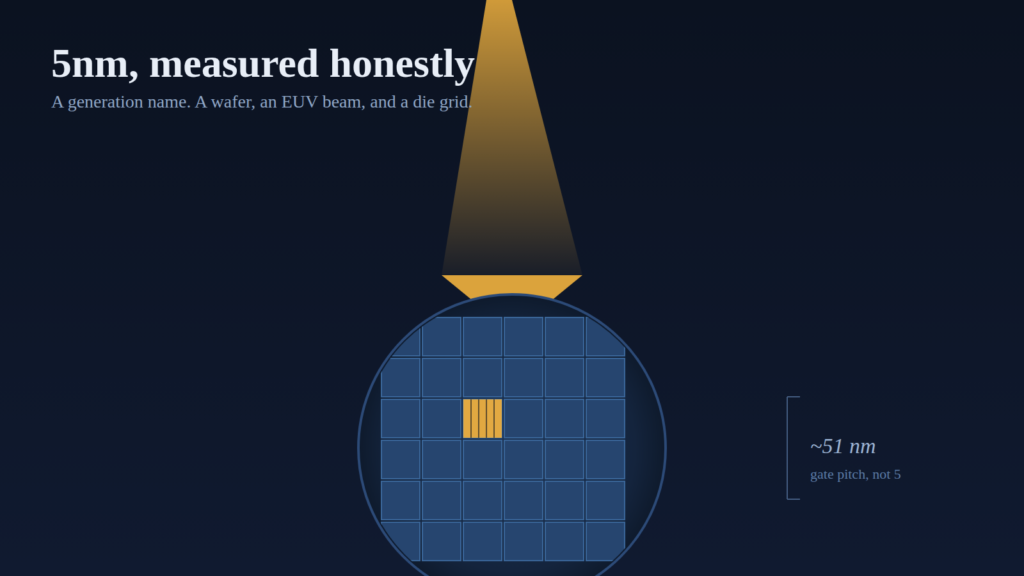
Illustration: Chips and Change (original artwork). A 300 mm wafer under an EUV light beam; the highlighted die is the one being exposed.
What “5nm” actually means
Nothing you can point to on the die. Node names stopped matching any physical dimension of the chip in the mid-1990s, when they became a marketing shorthand for “one step better than the last one”: the “130nm” nodes of that era actually had gates around 70nm (IEEE Spectrum, 2020). When Intel launched its 22nm FinFET in 2011, the gates measured about 26nm (IEEE Spectrum, 2020). For 5nm, expect a gate length around 18nm, a contacted gate pitch of about 51nm, and a tightest metal pitch near 30nm (Wikipedia, “5 nm process,” accessed 2026). For perspective, the smallest structures on a 5nm chip are still well over a hundred silicon atoms across.
So what does the name track? A generation of density and efficiency. TSMC told the 2020 IEEE IEDM conference that N5 offers 1.84 times the transistor density of its 7nm process (Wikipedia, “5 nm process,” accessed 2026). Real chips land short of that: teardown analysts measured the N5 high-density cell at about 137.6 million transistors per mm² against roughly 90.6 for N7, a real-world gain closer to 1.5 times (Angstronomics, 2022). Apple’s A14 averages about 134 million transistors per mm² (Wikipedia, “Apple A14,” accessed 2026). Compared to 7nm, TSMC quotes about 15% more speed at the same power, or about 30% less power at the same speed (Wikipedia, “5 nm process,” accessed 2026). Those are the real numbers behind the label.
Who makes 5nm chips
Three companies can, and only one of them does it the easy way.
TSMC defined the node with N5 in 2020 and stretched it through N5P, the N4 family, and Nvidia’s custom 4N variant (Design&Reuse, 2022). N5 was the first high-volume process built heavily on extreme ultraviolet lithography, using EUV on up to 14 layers of the process, against 4 or 5 layers on the improved 7nm nodes (Wikipedia, “5 nm process,” accessed 2026). N4 offers about 5% more speed or 10% less power over N5, and N4P pushes that to 11% more performance with 22% better power efficiency (Wikipedia, “5 nm process,” accessed 2026).
Samsung fabs a 5nm-class node for its own Exynos chips and some Qualcomm designs. Its 5nm-class wafers run about $13,000, 15 to 30% below TSMC’s (Silicon Analysts, 2026), but its 4nm-class successor measured only slightly denser than N5 on the die and arrived 16 months later, with yields that never matched TSMC’s (Angstronomics, 2022).
SMIC, China’s largest foundry, reaches 5nm-class density without EUV at all, using self-aligned quadruple patterning on older deep-ultraviolet machines (Tom’s Hardware, 2024). The trade-off is brutal: reported die costs up to 50% above TSMC’s, with yields around a third of TSMC’s (TrendForce, March 2025). It exists because export controls keep EUV tools out of China, not because it is economical; Huawei’s Ascend 910C is the best-known product of that effort (TrendForce, March 2025).
What actually ships on 5nm
The node carries a huge share of the world’s compute. Apple’s A14 was the first commercially available 5nm chip, announced in September 2020 in the iPad Air and shipping in the iPhone 12 that October, with 11.8 billion transistors (Wikipedia, “Apple A14,” accessed 2026). The same Firestorm-based family carried the M1, M1 Pro/Max and A15 through the Mac and iPad lines (Wikipedia, “Apple A14,” accessed 2026). On the PC and data-center side, AMD’s Zen 4 CPUs (Ryzen 7000) fab on N5, and Nvidia built its Hopper GPUs on the custom 4N variant (Wikipedia, “5 nm process,” accessed 2026; Design&Reuse, 2022). TSMC had to boost N5 output by around 25% in 2022 alone just to keep up with demand from AMD, Nvidia and MediaTek (Design&Reuse, 2022).
That breadth is the point: 5nm is where phone SoCs, laptop CPUs, and AI accelerators all meet.
5nm vs 7nm vs 3nm, in one table
| Node | Density (MTr/mm²) | Wafer cost (USD, 2026 est.) | Mask set (USD) | Typical products |
|---|---|---|---|---|
| 28nm | planar era | ~$3,000 | ~$1M | Analog, MCUs, power, automotive |
| 7nm (N7) | ~90.6 | ~$9,500 | ~$3.5M | Zen 2/3, A12/A13 |
| 5nm (N5/N4) | ~137.6 | ~$18,500 | ~$6.5M | A14–M2, Zen 4, Hopper |
| 3nm (N3E) | ~215 | ~$20,000 | ~$15M | A17 Pro, M3/M4 family |
Sources: density measurements from Angstronomics, 2022; wafer and mask costs are 2026 estimates from Silicon Analysts. The 28nm wafer price is the same figure we used in our 28nm article. Note that foundry pricing varies by customer and year: analysts tracking Apple’s actual payments have reported higher wafer prices at each node (Tom’s Hardware, January 2025).
Read the wafer column against the density column and the industry’s economics come into focus: 5nm buys you about 1.5 times the measured transistor density of 7nm for roughly twice the wafer price. Cost per transistor improved only modestly, and the era of chips getting reliably cheaper ended around 28nm anyway (Tom’s Hardware, 2024).
Why 5nm wafers cost so much
Three costs stack up. First, the wafer itself: TSMC N5/N4 runs about $18,500 per 300mm wafer in 2026 estimates, with a range of roughly $16,000 to $21,300 (Silicon Analysts, 2026). Second, the mask set: around $6.5 million before the first good die ships, against roughly $1 million at 28nm (Silicon Analysts, 2026). Third, the design: Silicon Analysts puts the total non-recurring engineering cost for a 5nm-class tape-out, masks included, at about $10 million, before years of design work (Silicon Analysts, 2026). One driver of the wafer price sits on the fab floor: EUV scanners cost more than $150 million, and 5nm spends many times more EUV passes per wafer than 7nm did (Silicon Analysts, 2026).
This is exactly why 28nm refuses to die. A $3,000 wafer with a $1 million mask set and modest design costs is the right answer for analog, power, automotive and industrial chips, as we argued in our 28nm deep dive. The leading edge is for parts that need the density: processors, GPUs, AI accelerators.
Is 5nm the right node for your chip?
Only if your chip is digital, dense and sold in volume. The decision rule from the fab floor is simple: multiply expected units by the die cost at each node, add the mask and design costs, and see where the total lands. A low-volume chip at 5nm pays for its mask set many times over before a single good die is sold; the same chip at 28nm or 16nm can be profitable from year one. And if you do go leading edge, the N4 derivatives are usually the sweet spot, since N4P delivers most of 3nm’s benefit at closer to 5nm’s wafer price (Wikipedia, “5 nm process,” accessed 2026).
FAQ
Is 5nm better than 7nm? Yes, in density and efficiency: TSMC claims 1.84 times the transistor density of N7, with real-world chips closer to 1.5 times, plus about 15% more speed at equal power or about 30% less power at equal speed (Wikipedia, “5 nm process,” accessed 2026; Angstronomics, 2022). But it is about twice the wafer price, so “better” depends on what your chip needs.
What does “5nm” mean in a chip? Nothing physically measurable. It is a generation name; the actual features, like a ~51nm gate pitch, are far larger than 5nm (Wikipedia, “5 nm process,” accessed 2026; IEEE Spectrum, 2020).
Who makes 5nm chips? TSMC (N5/N4), Samsung (5nm-class), and SMIC, which reaches 5nm-class density without EUV using quadruple patterning at much lower yields (Tom’s Hardware, 2024; TrendForce, March 2025).
Why are 5nm chips so expensive? The wafer costs about $18,500, the mask set around $6.5 million, and the total non-recurring engineering cost about $10 million before design labor (Silicon Analysts, 2026). Only high-volume products can spread those costs.
Is 4nm better than 5nm? TSMC’s N4 family is an incremental evolution of N5, not a new node: N4 offers about 5% more speed or 10% less power over N5, and N4P about 11% more performance with 22% better power efficiency (Wikipedia, “5 nm process,” accessed 2026).
The Chips and Change Team covers the semiconductor industry from the fab floor up. Read next: Why 28nm still rules the world.