


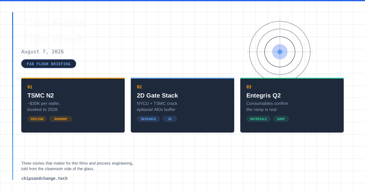
Another week where the leading edge got more expensive and the research floor got more interesting. Three stories with real process implications: TSMC’s N2 pricing crossing $30,000 a wafer, a gate-stack breakthrough for 2D channels out of NYCU and TSMC Corporate Research, and an earnings print from the consumables layer that confirms the ramp is real.
TSMC’s N2 Wafer Hits ~$30,000, and the Order Book Runs to 2028
What happened: TSMC’s 300mm N2 wafers are now priced around $30,000 each, up from $18,000 to $20,000 at N3, with N2 and A16 capacity booked out to 2028 while 3nm wafer starts climb toward 180,000 a month by early Q4, two to three months ahead of schedule (tech-insider.org; TrendForce).
Thin films take: The headline read is supply and demand, and that is true. But the node-to-node jump is mostly a film-stack story. A GAA wafer carries more deposited layers than any FinFET: conformal ALD wrapping four nanosheet channels, inner spacers, a TiN work-function metal now tuned per device instead of per node, low-k spacer films, and the superlattice epi the channels are etched out of. Film count per wafer has roughly doubled since N5. TrendForce’s pushback, that the real increase is closer to 10 to 20 percent once customer tiers are counted, matches what I see on the floor: the added cost is deposition and etch time, not litho. And A16 at a rumored $45,000 adds backside power delivery, which means carrier bonding, a backside grind, and an entire backside film stack with re-passivation. Wafer bow from those thick backside films will be the next yield fight, and the teams that control stress in the dielectric stack will earn their keep.
NYCU and TSMC Crack the 2D Gate Stack with an Epitaxial AlOx Buffer
What happened: Researchers at National Yang Ming Chiao Tung University and TSMC Corporate Research demonstrated monolayer MoS2 top-gate transistors combining a gate dielectric with about 1nm equivalent oxide thickness and 0.45 mS/um maximum transconductance, using an epitaxial aluminum layer on CVD-grown MoS2 oxidized into a 0.42nm AlOx buffer under HfO2 (SciTechDaily; Nature Electronics).
Thin films take: This is the nucleation problem I have fought for a decade. A 2D channel has no dangling bonds, so ALD on MoS2 nucleates in islands: pinholes, interfacial charge, mobility collapse. We have tried ozone pulses, plasma pretreats, and polymer seeds, and the EOT, control, and transport triangle never closes. The NYCU move is elegant because a metal wets the van der Waals surface epitaxially, and oxidation gives a self-limiting, atomically smooth AlOx that HfO2 can actually grow on. 0.42nm of buffer under high-k, about 1nm EOT, low hysteresis, 0.45 mS/um on a 100nm channel: that combination has been the blocker for 2D logic. And the channel is CVD-grown monolayer, not an exfoliated flake, so there is a wafer-scale path. An oxidized epitaxial metal may be the seed layer that makes 2D gate stacks manufacturable, the kind of interface work that decides whether MoS2 ever reaches a high-volume line.
Entegris Q2: The Consumables Layer Confirms the Ramp Is Real
What happened: Entegris beat across the board with $883.2M in Q2 revenue, up 11% year over year, and adjusted EPS of $0.93, up 41%, as AI demand reached the materials layer: Advanced Purity Solutions grew 17% to $514.6M with margin expanding 620 basis points to 30.3%, and Q3 was guided to $905M to $935M (Tech Times).
Thin films take: Materials suppliers are the canary in the fab. Entegris is roughly 95% consumables: deposition precursors, filtration membranes, CMP slurries, specialty gases. When that book grows 11% and EPS grows 41%, the mechanism is fab utilization showing up in the BOM, not hype. The compounding driver is content per wafer. GAA at N2 means more ALD steps, so more precursor drums, more filter change-outs, more slurry per wafer. HBM stacks add TSV barrier deposition and dielectric fill, and every one of those steps runs a qualified material with years-long switching costs baked in. I have lived those qualifications; once a membrane is in the flow, you do not swap vendors mid-ramp. Per-wafer materials consumption, not wafer count, is the growth curve to watch this cycle, and it is still climbing.
RELATED POSTS
View all