

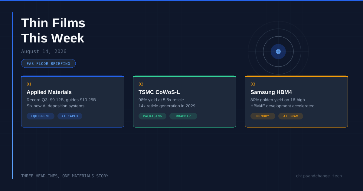
This week the money moved through the machines. Applied Materials printed a record quarter on AI deposition demand, TSMC pushed CoWoS-L to 98 percent yield at 5.5x reticle, and Samsung crossed the golden-yield line on HBM4. Three business headlines, and each one is a thin films story underneath.
Applied Materials: Record Quarter, Six New AI Systems, and a Margin Grumble
What happened: Applied Materials posted record Q3 revenue of $9.12B with earnings above estimates and guided Q4 to $10.25B, yet shares fell about 5 percent as investors wanted faster growth from the AI equipment winner; the company also introduced six new systems for AI chipmaking (Reuters; 24/7 Wall St.).
Thin films take: I have watched Applied Materials’ order book long enough to remember when a billion-dollar deposition quarter was an event. Now it is a baseline. Record $9.12B, a $10.25B guide, six new systems for AI chipmaking: Endura-class PVD and Producer-class CVD being pulled through the door by GAA and backside power delivery. The margin grumble, 50.4 percent gross and flat, misses the point. Mix shifts as AI logic pulls in more ALD and high-aspect-ratio CVD, and the new systems target the film stacks that decide N2 yields: conformal metal gates, low-k spacers, the thick dielectric build on the backside. When the deposition house prints record quarters two years into a node transition, film count per wafer is still climbing. The AI buildout has become a materials-engineering capex story, and deposition is the biggest line item in it.
TSMC Hits 98% Yield on CoWoS-L at 5.5x Reticle, 14x Comes in 2029
What happened: TSMC has reached 98 percent yield on CoWoS-L interposers at 5.5x reticle size, with a 14x reticle generation on the roadmap for 2029 (TechPowerUp).
Thin films take: CoWoS-L at 5.5x reticle is not a packaging headline, it is a thin films achievement. A reticle-scale interposer means one RDL field with Cu lines and SiO2 or polymer dielectric that has to stay uniform across an area that used to be five separate die. At that scale the yield killers are film thickness spread, Cu plating nodulation, and dielectric pinholes, not litho. 98 percent says the dielectric deposition and CMP are holding flatness and defectivity across the whole field, and that the stitching boundaries are invisible to plating. The 14x jump in 2029 will stress every deposition and planarization step again, and hybrid bonding on top means the top dielectric surface becomes the device. 98 percent at 5.5x reticle is a dielectric uniformity and CMP story, and 14x in 2029 is the next stress test.
Samsung Reports 80% “Golden Yield” on HBM4, Accelerates HBM4E
What happened: Samsung has reportedly hit an 80 percent “golden yield” on HBM4 production as it pushes to take AI DRAM share from SK Hynix, and is speeding up HBM4E development (Wccftech; Seoul Economic Daily).
Thin films take: Golden yield on HBM4 is a stack-level statement, but the work is all films and interfaces. A 16-high stack carries thousands of TSVs, and each one needs a TaN/Ta barrier and Cu seed that PVD lays down void-free, plus a dielectric fill that does not crack. The step that usually owns HBM yield is the bond interface: MR-MUF with NCF for the bulk, with hybrid bonding creeping in from the base die as HBM4E ramps. 80 percent means deposition and planarization are playing at DRAM-grade defect densities across 16 die, and that film-stack warpage is under control through reflow. Samsung speeding up HBM4E says they trust the film work enough to compress the product cycle. 80 percent on 16-high means the TSV fill and the bond interface are both qualified at volume, and the rest is a market share question.
RELATED POSTS
View all