


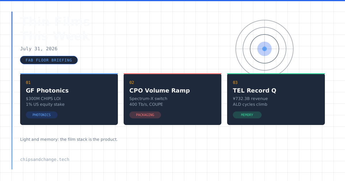
Welcome to this week’s Fab Floor Briefing: three stories that matter for thin films and process engineering, told from the cleanroom side of the glass. This week is all about light and memory, two businesses where the film stack is the product.
1. Washington Buys Into GlobalFoundries’ Photonics Bet: $300M CHIPS LOI, 1% Stake, CPO Front and Center
What happened: GlobalFoundries signed a letter of intent with the US Department of Commerce for a $300 million CHIPS R&D award to accelerate its silicon photonics program, with the government taking a 1% equity stake and the work emphasizing co-packaged optics for AI data centers.
Thin films take: Silicon photonics is a thin films business wearing a chip company’s clothes. The passive backbone is a PECVD silicon nitride core in a silica cladding, and the receiver side is selective germanium epitaxy in oxide windows for the photodetectors. I’ve run 300 mm SiPh flows, and the pain is never the waveguide itself, it’s the thermal budget: you deposit and anneal these films after the FEOL dopants are already in, so the reflow tricks from interlevel dielectric work are off the table. The government taking equity tells me Washington now treats photonics capability the way it treats fabs, as a national-security asset. For process engineers that means funded lines for SiN deposition, Ge epi, and edge-coupler CMP on GF’s 45 nm SOI platform. Waveguide loss is the yield metric that matters: every 0.1 dB/cm shaved in the PECVD nitride is capacity you never have to build.
Source: SiliconANGLE · Semiconductor Digest
2. CPO Crosses Into Volume Ramp, and the Optical Engine Becomes a Yield Problem
What happened: TrendForce reports NVIDIA has begun shipping its Spectrum-X CPO switch, co-developed with TSMC using COUPE packaging and rated up to 400 Tb/s, while Broadcom volume-ramps its 51.2T Bailly switch, with optical engine yield, silicon photonics fab capacity, and advanced packaging availability flagged as the three bottlenecks to expansion.
Thin films take: Every CPO roadmap hits the same wall: the optical engine is a thin films stack with a laser bolted on. You’re hybrid-bonding a photonics die to the switch ASIC, and the bond interface is Cu pads on SiO₂, which means the whole package lives or dies on CMP. One micro-scratch, one dishing hotspot on the bonding surface, and that die is scrap before it ever sees light. I’ve watched die-to-wafer hybrid bonding teams chase particle specs that would make a logic fab blush: a single 0.5 µm defect on the bond surface can kill the optical path, and there is no rework. Add laser arrays dumping heat next to the switch, and the underfill and lid materials start dictating the package design. Hybrid bonding surface prep is where CPO yield goes to die: one micro-scratch in the oxide and that optical engine is a light fixture, not a transceiver.
Source: TrendForce
3. TEL’s Record Quarter Says the Memory Film Stack Isn’t Done Growing
What happened: Tokyo Electron posted record revenue of ¥732.3 billion in FY2027 Q1 (April through June 2026) and raised its first-half net profit forecast to ¥349 billion on July 30, citing AI data center investment and strong memory chip demand.
Thin films take: For anyone who thinks memory capex has peaked, TEL’s numbers are the tell. A record quarter built on DRAM and HBM demand means one thing from where I sit: more ALD cycles. Every DRAM generation pushes the capacitor higher in aspect ratio and the high-k stack thinner, and the word line keeps eating tungsten. Those are deposition-intensive structures, and TEL’s Triase ALD and CVD line is the default answer for a big share of them. HBM adds its own film tax: TSV liners, tungsten fill, backside redistribution. I’ve lived through three memory supercycles, and the tool that sells first in an AI-driven upcycle is always the deposition tool, because every bit of new memory capacity is a film stack first, and TEL’s beat-and-raise says the deposition content per wafer is still climbing.
Source: DigiTimes · Investing.com
That’s the floor for this week. Keep your precursors cold and your ellipsometer calibrated.
RELATED POSTS
View all