Every AI accelerator shipping today is memory-constrained, and the part it runs out of first is not logic or lithography but a thumb-sized stack of DRAM dies bonded on top of a logic die. High Bandwidth Memory has gone from a niche JEDEC specification to the single most contested product in the semiconductor industry: three memory makers fighting over it, a foundry pulled into its base dies, contract prices forecast to rise 121% in 2027, and capacity that cannot be added fast enough. This Deep Dive is a review of HBM from the fab floor up: how the stack is actually built, who builds it, what the data shows, where the technical disagreement sits, and what to watch next.
Why HBM matters now
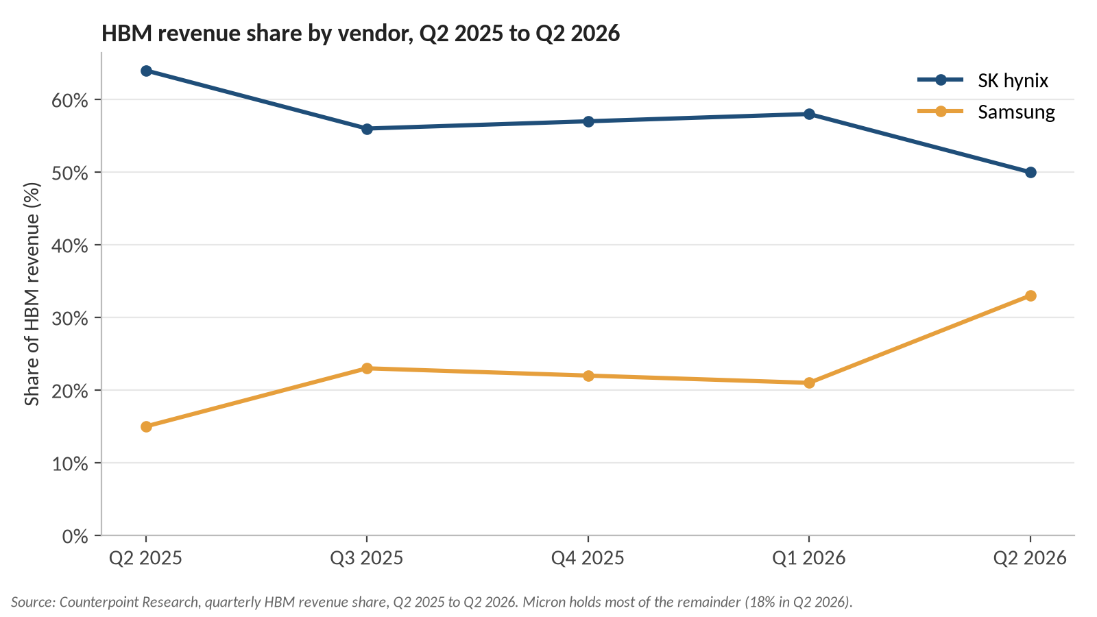
Three numbers frame the moment. First, market structure: in Q2 2026, SK hynix held 50% of HBM revenue by Counterpoint Research’s count, Samsung 33%, and Micron 18% — and SK hynix’s lead fell from 58% in a single quarter as Samsung’s HBM4 ramp took hold. Second, price: TrendForce raised its 2027 blended HBM ASP forecast to a 121% year-over-year increase, on supply constraints, a richer HBM4 mix, and the HBM4E ramp arriving in the second half of 2027. Third, the wider memory market those numbers sit inside: TrendForce now projects the global memory market at $889.3 billion in 2026 and more than $1.28 trillion in 2027, with HBM the fastest-growing slice.
The fab-floor translation: HBM is where DRAM process control, advanced packaging, and logic foundry work collide in one product. A fab that can print DRAM cells cannot necessarily ship HBM, because the hard part is not the memory array — it is thinning twelve dies to a few tens of microns each, etching thousands of through-silicon vias in them, and bonding the stack with cumulative warpage under control. That is why capacity additions take years and why this week’s announcements (the week of November 16, 2026) — Micron moving first equipment into its Singapore HBM packaging plant, SPIL committing to triple advanced packaging capacity by 2029 — are the real supply forecast. Both were covered in Friday’s Fab Floor roundup.
How HBM works
HBM inverts the usual DRAM trade. Conventional DDR5 gets capacity per module but is pinned at the edges; its bandwidth is limited by the number of I/O balls a package can physically carry. HBM gets bandwidth by going vertical: 4 to 16 DRAM dies are stacked on a base logic die, connected by through-silicon vias (TSVs) that pass through each die’s active layer, and the whole stack talks to the host processor over a very wide interface through a silicon interposer or bridge.
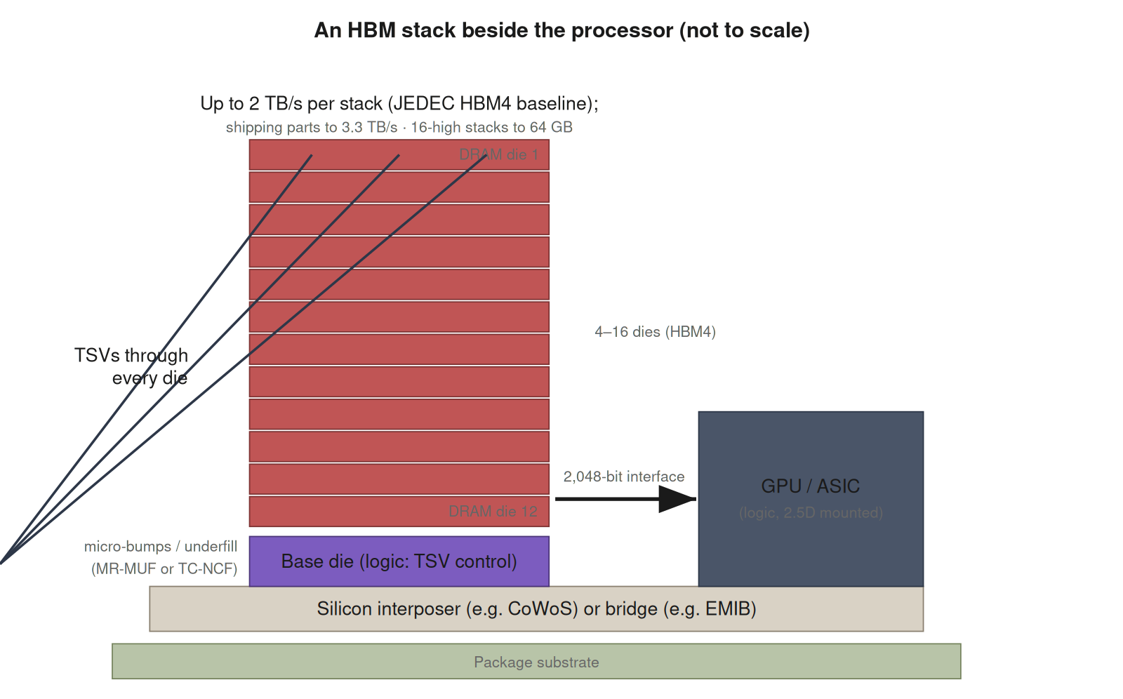
SK hynix’s 2017 IEEE International Memory Workshop paper remains the cleanest architecture survey: stacked DRAM dies over a base die, TSV and die-stacking technology, bandwidth above 256 GB/s per stack at a time when that was the breakthrough, and a first accounting of the packaging challenges — reliability and thermal dissipation — that still define the product today.
The generational ladder since then has been steady interface work plus steady stacking work. Samsung’s HBM2E generation (ISSCC 2020) pushed a 16 GB stack to 640 GB/s with data-bus window extension and on-die ECC. SK hynix’s HBM3 (IEEE JSSC 2022) reached 192 Gb and 896 GB/s in a 12-high stack, adding TSV auto-calibration, symbol-correcting in-DRAM ECC, and machine-learning-based layout optimization — the base and core dies now exchange so much data, so fast, that the TSVs themselves need calibration schemes. HBM3E raised pin speeds further; and HBM4, standardized as JEDEC JESD270-4 in April 2025, is the architectural break: the interface doubles to 2,048 bits across 32 independent channels (64 pseudo-channels), the baseline pin speed is 8 Gb/s for 2 TB/s per stack, stacks run 4-high to 16-high on 24 Gb or 32 Gb dies, and maximum capacity reaches 64 GB per stack.
The less advertised HBM4 change is the process split. Through HBM3E, the base die was a memory-maker’s own logic process. HBM4’s base die carries real logic — physical layer work, and increasingly customer-specific functions — and the industry has split it from the DRAM core dies: SK hynix adopted TSMC’s 12nm-class process for its HBM4 base die, and Samsung built its 12-high, 36 GB, 3.3 TB/s HBM4 stack (ISSCC 2026) on 6th-generation 10nm-class DRAM core dies paired with a Samsung Foundry 4nm base die. The memory company still owns the stack; a foundry now owns the brain.
How a stack is actually made
From the floor, an HBM line is a sequence of yield-critical steps that did not exist in a conventional DRAM fab. The DRAM dies are fabricated, then thinned to tens of microns. TSVs are etched and filled through the active silicon. The dies are stacked over the base die with micro-bumps, joined by thermal compression bonding (TCB), and the gaps between dies are filled — SK hynix’s mass-reflow molded underfill (MR-MUF) approach versus Samsung’s thermally-compressed non-conductive film (TC-NCF) is a long-running materials dispute in its own right. The finished stack is then mounted beside the GPU or ASIC on a silicon interposer — TSMC’s CoWoS, whose fifth-generation version stretched the interposer to 2,500 mm² in 2021 — or, on Intel’s parts, onto an embedded multidie interconnect bridge (EMIB), which localizes the high-density interconnect instead of spreading it across a full interposer.
HBM4 makes every one of those steps harder. SK hynix’s package-development paper at the 2026 VLSI Technology and Circuits Symposium (their MTV4 test vehicle) reports the specifics: 12-layer stacking with die thickness and gap height pushed down until die warpage and gap fill become the limiting physics, and micro-bump joint integrity that must hold across the entire 12-layer stack. The tool side is responding in kind — Kulicke & Soffa’s fluxless thermocompression bonding systems, shipped to two Taiwan customers this month, attack the flux-residue yield problem at fine pitch, and the A*STAR/Applied Materials hybrid-bonding work presented at ECTC 2026 demonstrated copper/dielectric bonding below 250°C, low enough to survive the temperature budgets of a fully populated stack.
Who the players are
Three memory makers build HBM, and the 2026 story is the reshuffling among them. SK hynix built its lead on early HBM3E qualification with NVIDIA and still leads with 50% of HBM revenue in Q2 2026, but TrendForce reported interface-sync issues pushed its HBM4 mass production to Q3 2026, with capacity redirected to DDR5 and LPDDR5 in the meantime. Samsung moved first on HBM4: it completed validation and began shipments in Q2 2026 onto NVIDIA’s Rubin platform, said on its Q1 2026 earnings call that its HBM4 volume was already sold out for the year, and by late August was cited at roughly 80% HBM4 yield — which is how its share jumped from 21% to 33% in one quarter. Micron holds the remaining 18%, entered HBM later but secured allocation with several AI chip vendors, moved first equipment into its Singapore HBM packaging facility for 2027 production, and in September announced work with NVIDIA on what it calls the industry’s first custom HBM4E, named NVHBM.
The foundries are players now too. TSMC supplies SK hynix’s HBM4 base dies and, per October reporting, will supply 3nm base dies for NVIDIA’s NVHBM custom stacks — drawing all three memory makers into TSMC’s orbit for the logic layer of a memory product. Samsung keeps its base dies in-house on its own 4nm foundry process. And the packaging houses — SPIL, ASE, Amkor — own the bump, assemble, and test capacity that TrendForce expects to stay supply-constrained through 2027.
What the data shows
The JEDEC specification and the shipping parts have already diverged, which tells you where the engineering is going. The standard’s baseline is 8 Gb/s per pin and 2 TB/s per stack; the parts being qualified run well past it — Samsung’s HBM4 at up to 3.3 TB/s per stack on 11.7–13 Gb/s pins, Micron above 2.8 TB/s on pins above 11 Gb/s, SK hynix above 10 Gb/s. TrendForce expects 2026 HBM shipments to exceed 30 billion Gb, with HBM4 overtaking HBM3E in the second half of the year and making up roughly 55% of 2026 HBM revenue; Samsung said HBM4 would exceed half of its HBM revenue starting in Q3 2026. Demand per part is climbing too: TrendForce puts HBM capacity per AI ASIC at 216–288 GB in 2026, rising to 384 GB per GPU on Rubin Ultra in 2027.
The price data is the clearest signal of scarcity. HBM contract prices are forecast to surge multiples higher in 2027, with the blended ASP up 121% year over year, because standard-DRAM prices have been rising since the second half of 2025 and HBM capacity crowds out conventional DRAM capacity on the same wafers — the DRAM squeeze covered in Tuesday’s CXMT post. Bit supply is expected to grow only 50–60% in 2027 against demand that exceeds it — which is why NVIDIA is reportedly evaluating lower-stack (8-high) HBM4 for Rubin Ultra, trading capacity per stack for availability, with 8-high stacks expected to carry a 10–20% premium per gigabit over 12-high parts.
Where the disagreement is
A review article owes you the open technical arguments, and HBM has three.
Hybrid bonding versus micro-bump TCB. Today’s stacks are joined with solder micro-bumps under thermal compression. The case against them was made plainly in the Xperi/ECTC 2019 paper: TCB throughput is low, and the process cannot scale below about 40 μm pitch, which caps how many TSV connections a stack can carry. Hybrid bonding — direct copper-to-copper bonds in dielectric, no solder — removes the pitch floor and the flux. The counter-case is industrial: TCB and MR-MUF are qualified at 12- and 16-high stacks today, while hybrid bonding for memory is still being proven, layer by layer, with thermal stability and grain-size control as the open problems (the A*STAR 2026 work is representative). The 2025 review literature in Electronics frames the stakes precisely: conventional fixes — heat spreaders, microchannels, high-density TSVs, MR-MUF — lower but do not eliminate internal thermal resistance, which rises sharply beyond 12-layer stacks. My read from the floor: hybrid bonding arrives for HBM4E and custom parts first, where the pitch demand is most acute, while commodity HBM4 stays on TCB through the 2027 capacity crunch — nobody retools their qualified line mid-shortage.
Thermals as the real stack-height limit. The DRAM industry can build 16-high stacks; the question is whether it should. Samsung’s own thermal simulations of custom HBM (ECTC 2024) show twelve DRAM dies stacked directly on a customer-specific logic die create thermal-management challenges the logic die’s own TDP compounds. IMEC’s IEDM 2025 work on HBM-on-GPU integration evaluates base-die removal and DRAM-die merging as co-optimization levers — the radical suggestion being that the base die itself is becoming thermally expendable. Georgia Tech’s memory-on-logic work claims 64× throughput and 3× energy-efficiency gains from stacking HBM directly on compute, if and only if the heat can be moved. And a JSTS finite-element study quantifies the intuition every process engineer carries: thermal dissipation degrades non-linearly as DRAM layers are added. The disagreement is not whether thermals bind; it is whether the industry solves them with packaging (heat spreaders, microchannels, backside paths) or with architecture (fewer, fatter layers, lower stacks, or moving compute into memory).
Standard versus custom base dies. HBM4’s logic-rich base die opened a fork in the road. The custom path — NVIDIA’s NVHBM, Samsung’s custom samples targeted for 2027, SK hynix’s own custom-HBM concept — puts customer logic in the memory stack and pulls foundries into the loop, with TSMC’s GUC partnership detailing an N3P base die for custom HBM4E at 12.8 gigatransfers per second. The standardization counter-argument is about yield and cost: a University of Rochester/ISQED 2026 study models active interposers — folding base-die logic into a shared interposer — and finds the yield economics depend heavily on node and stack count. Custom HBM sells performance; standard HBM sells availability. In a supply-constrained 2027, availability is not a small thing.
What to watch next
Four markers for the next twelve months. HBM4E: pin speeds of 14–16 Gb/s and stack bandwidths of 3.6–4.0 TB/s are the vendor targets, with Samsung and SK hynix both pointing at 48 GB 12-high parts — watch whether the interface work survives contact with the thermal budget. Custom HBM: Samsung’s customer samples in 2027, Micron’s NVHBM, and SK hynix’s custom line will show whether the base die becomes a product differentiator or a commodity TSMC slot. Bonding: the first memory product shipping with hybrid bonding is the inflection to watch for, and the low-temperature bonding papers coming out of ECTC and VLSI are the leading indicator. And capacity: Micron’s Singapore plant in 2027, SK hynix’s M15X and Yongin Phase 1, and the packaging houses’ build-outs decide whether TrendForce’s 121% ASP forecast holds or softens. If 2026 was the year HBM4 arrived, 2027 is the year the industry finds out whether stacked DRAM is a product or a bottleneck wearing a product’s name.
TL;DR
HBM stacks 4–16 thin DRAM dies on a logic base die over TSVs and a wide interface, and it is now the binding constraint on AI compute: SK hynix holds 50% of a market growing fast enough that 2027 blended prices are forecast to rise 121%, with Samsung at 33% after the fastest HBM4 ramp on record and Micron at 18%. HBM4 doubled the interface to 2,048 bits and split the base die out to foundry logic processes. The open fights are hybrid bonding versus micro-bump TCB, thermals versus stack height beyond 12 layers, and standard versus custom base dies. What to watch: HBM4E at 14–16 Gb/s, custom HBM samples in 2027, the first hybrid-bonded memory product, and the Singapore and Yongin capacity ramps.
FAQ
What is High Bandwidth Memory in simple terms?
A stack of 4 to 16 thin DRAM dies sitting on a logic base die, connected vertically by through-silicon vias and horizontally to the processor by a very wide interface (2,048 bits in HBM4). Going vertical is what buys the bandwidth: up to 2 TB/s per stack under the JEDEC HBM4 standard, with shipping parts exceeding that.
How does HBM4 differ from HBM3E?
The interface doubles from 1,024 to 2,048 bits, channels double to 32, and the base die moves to an advanced logic process — SK hynix uses TSMC’s 12nm-class process, Samsung its own 4nm. The JEDEC baseline is 8 Gb/s per pin and 2 TB/s per stack; shipping parts run to 3.3 TB/s.
Who makes HBM?
SK hynix (50% of Q2 2026 HBM revenue), Samsung (33%), and Micron (18%), per Counterpoint Research. TSMC and Samsung Foundry supply the base dies, and packaging houses like SPIL, ASE, and Amkor provide the bump, bond, and test capacity.
Why is HBM so expensive?
It crowds out conventional DRAM capacity, its packaging yield is the hard part rather than the memory array, and demand exceeds bit supply — TrendForce forecasts 2027 bit supply growth of only 50–60% and a blended HBM ASP up 121% year over year.
Will hybrid bonding replace micro-bumps in HBM?
Eventually, partially. Micro-bump TCB is qualified at 12–16 layers today and nobody retools a qualified line mid-shortage, but the pitch and throughput limits are real, and low-temperature copper/dielectric hybrid bonding demonstrated below 250°C is the leading candidate for HBM4E and custom parts.