

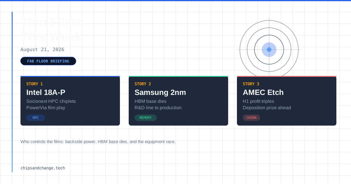
Three stories this week, and each one is really about who controls the films. Intel signed a serious HPC chiplet customer onto 18A-P, Samsung is pushing HBM base dies to cutting-edge nodes and paying for it with foundry capacity, and China’s AMEC tripled its profit on etch tools while the deposition prize stays out of reach. Same materials physics underneath, three different fabs.
Intel Lands Socionext for 18A-P High-Performance Compute Chiplets
What happened: Japanese custom-SoC house Socionext will build high-performance compute chiplets on Intel’s 18A-P process, adding Intel Foundry as a second source alongside TSMC, and its shares slid more than 5 percent as investors weighed the economics of the deal (New Electronics, TrendForce, digitimes).
Thin films take: For those of us who have spent years qualifying backside power, 18A-P is the process I point to when people ask what actually changed at Intel. The ribbonFET channels are demanding enough: conformal ALD of the high-k stack and TiN work-function metal across four or five stacked nanosheets, with precursor depletion fighting you at the bottom of the stack. But PowerVia is the film play. You grind the wafer, etch through the substrate, and build a second interconnect network on the backside, which means thick stress-balancing dielectrics, deep via fills, and a wafer that wants to bow every way at once. The yield limiter on backside power was never litho, it was film stress and wafer flatness. A designer like Socionext signing off on 18A-P for chiplets says Intel’s backside stack is finally stable enough to bet a product on. 18A-P’s credibility rests on a backside film stack that stays flat enough to keep every subsequent litho level in focus.
Samsung Repurposes an R&D Line for 2nm HBM Base Dies
What happened: Samsung is reportedly converting a foundry R&D line into production capacity targeting cutting-edge 2nm HBM base dies in anticipation of future NVIDIA demand, extending its 4nm HBM4 base-die roadmap, and will break ground on a KRW 6 trillion Onyang HBM fab in September (TrendForce, Wccftech, TrendForce).
Thin films take: The HBM base die is quietly becoming the most interesting film stack in memory, because it is logic-class BEOL bolted onto a DRAM supply chain. Moving it to 2nm means finer pitches, lower-k dielectrics, and a lot more ALD content, all on a wafer that will later be ground to tens of microns, punched with TSVs, and bonded. Everything downstream lives or dies on stress engineering: the BEOL films have to survive backside grind without cracking, the TSV barrier and seed have to go down void-free, and the top Cu-in-dielectric bond surface has to be flat within nanometers so the oxide-to-oxide bond wets out. Repurposing an R&D line tells me Samsung is compressing the qual cycle, proving the 2nm base-die process before Onyang breaks ground. Film stress and wafer warpage, not transistor performance, are what gate the 2nm HBM base die.
AMEC Triples H1 Profit as China’s Etch Beachhead Grows
What happened: China’s AMEC reported first-half net profit tripling to 2.83 billion yuan with plasma-etch profit nearly doubling, and announced a 3.5 billion yuan Phase II expansion of its Lingang industrialization base, as its tools gain share in Chinese fabs while TSMC phases them out (Moomoo, finance.biggo, Tech Times).
Thin films take: I have watched AMEC go from the MOCVD supplier nobody wanted to the etch vendor Chinese fabs actually depend on, and this week’s numbers say the transition is working. Tripling first-half profit on plasma etch, with SMIC having bought 800-plus machines, is the beachhead. But here is what gets my attention as a films person: etch was always the easier entry point, the real prize in equipment localization is deposition, and AMEC’s roadmap has been creeping from etch into CVD, ALD, and epitaxy for years. The 3.5 billion yuan Lingang Phase II spend is them scaling the industrialization base to chase exactly that. TSMC phasing AMEC tools out of its fabs is the market telling them they are not yet a front-end films house, and that gap is measured in film uniformity, defect density, and process control data that takes years to accumulate. China’s equipment localization story is an etch story today, but the deposition prize is what the Lingang expansion is really buying.
RELATED POSTS
View all