Author: Herm

  • Thin Films This Week — May 22, 2026

    Thin Films This Week — May 22, 2026

    1. Intel 18A Yields Hit 7–8% Monthly Improvement; 14A ‘Holy Grail’ PDK 0.9 Due October 2026

    What happened: Intel CEO Lip-Bu Tan announced 18A process yields are improving 7–8% per month—the industry standard cadence—and confirmed 14A PDK 0.9 is on track for October 2026, calling it “the Holy Grail” for external customers, while warning engineers they’ll be fired if chips exceed B0 stepping. (Wccftech)

    Thin films take: I’ve been in process integration long enough to know that 7–8% monthly yield improvement on a debut GAA node is—if real—genuinely impressive. RibbonFET’s stacked nanosheets demand atomic-layer precision across a much larger effective gate perimeter than FinFET ever did. Every one of those horizontal channels needs conformal gate oxide, work-function metal, and high-k dielectric deposition that’s uniform top-to-bottom across the entire sheet stack. That’s an ALD challenge FinFET never posed. PowerVia adds another thin-films headache: backside metal deposition and planarization at a scale we’ve never done in production. The B0 stepping discipline matters because each mask respin on a GAA node costs months and millions. If Tan is serious about first-pass A0, he’s betting that his deposition and etch teams can deliver process windows tight enough—and stable enough—that the design-technology co-optimization doesn’t break between tapeout and first silicon. I’ll believe 14A risk production in 2028 when I see a fully qualified high-volume ALD process for sub-1.5nm-class gate dielectrics that doesn’t require three reworks per wafer lot.

    2. EV Group to Demo Hybrid Bonding, IR LayerRelease at ECTC 2026—Enabling Sub-Micron 3D Stacking

    What happened: EV Group (EVG) announced it will showcase its latest hybrid bonding (wafer-to-wafer and die-to-wafer), IR LayerRelease technology for nanometer-precision layer transfer through silicon, and maskless lithography at ECTC 2026, including a joint paper with Intel on high-speed bond overlay measurement. (EV Group)

    Thin films take: This is the story that most directly affects what we do in the cleanroom every day. Hybrid bonding is fundamentally a thin films problem masquerading as a packaging problem. You’re asking two dielectric surfaces—typically SiOₒ deposited by PECVD or PVD—to fuse at low temperature with sub-micron alignment and zero voids across a 300 mm interface. The dielectric deposition uniformity, surface roughness, and plasma activation chemistry determine whether you get a bond that passes CMP or a rejected stack. EVG’s IR LayerRelease is particularly interesting: using an IR laser through silicon with inorganic release materials eliminates the glass carrier and its associated thermal budget constraints, which means you can transfer thinner device layers without warpage. For those of us who’ve spent years fighting carrier-glass CTE mismatch on 3D NAND and CMOS image sensor stacks, this is a genuinely useful trick. The Intel co-authored metrology paper matters too—bond overlay measurement at production speed has been the gating item for die-to-wafer hybrid bonding. If EVG’s overlay metrology breaks 100 nm at production throughput, that’s the unlock that makes chiplet stacking cost-effective at scale.

    3. Samsung Strike Averted at 11th Hour—But Foundry Yield Concerns Remain

    What happened: Samsung Electronics and its largest labor union reached a tentative wage deal just 90 minutes before a planned 18-day general strike by 48,000 workers was set to begin on May 21, with the deal now subject to a worker vote through May 28. (Korea JoongAng Daily)

    Thin films take: From a process engineer’s perspective, the strike was a distraction from a deeper problem: Samsung’s SF2 (2nm GAA) yields are rumored to be stuck around 50–60%, versus TSMC’s N2 at 80%+. The labor situation matters because you can’t fix a yield problem if 48,000 people aren’t on the fab floor. But the real thin films issue here is that Samsung was first to GAA production with SF3E in 2022—three full years ahead of everyone else—and they still haven’t cracked the deposition uniformity challenge across their nanosheet stacks. GAA yields live or die on conformal ALD of high-k dielectrics and metal gate work-function layers inside those horizontal channels. If your ALD step coverage falls below 95% on the bottom-most sheet, you’re looking at threshold voltage shifts that kill die sort yields across the whole wafer. Samsung’s 2nm yields being stuck where TSMC’s were 18 months earlier suggests the gap isn’t just in patterning—it’s in deposition and etch precision at the atomic layer level. Until Samsung demonstrates a qualified high-volume ALD process for 2nm-class GAA that matches TSMC’s film uniformity, the foundry market stays a one-horse race regardless of labor peace.

  • Thin Films This Week — May 15, 2026

    Thin Films This Week — May 15, 2026

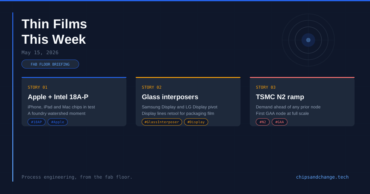
    🍏 1. Apple Confirms Intel 18A-P Testing for iPhone, iPad, and Mac Chips — A Foundry Watershed

    What happened: Multiple reports this week confirm Apple is actively testing Intel’s 18A-P process node at Fab 52 in Chandler, Arizona, with analyst Ming-Chi Kuo detailing small-scale 2026 testing, a 2027 ramp for M7-series chips, and potential 14A production for iPhone chips by 2028 — backed by a preliminary agreement reported by the Wall Street Journal on May 9.

    Thin films take: I’ve been doing this long enough to remember when Intel was the unquestioned king of thin-film process control, back when everyone else was still trying to figure out hafnium-based high-k. The 18A process stack is no joke — RibbonFET GAA nanosheets with PowerVia backside power delivery means you’re depositing dielectric layers and metal fills on both sides of the wafer. That’s a fundamentally different challenge for every PECVD and PVD chamber in the line. The 18A-P variant reportedly optimizes for mobile power envelopes, which tells me they’ve tuned the interlayer dielectric (ILD) stack and contact resistance through specific ALD high-k/metal gate (HKMG) process changes. For those of us in process integration, the bigger story is what this means for deposition tool utilization at Intel’s Arizona fabs — AMAT Endura and Lam Kiyo chambers are going to be running triple shifts. The key question no one’s asking yet: how does PowerVia affect stress management in the thin-film stack? Backside processing completely changes the stress asymmetry budget.

    Sources: MacRumors, WCCFTech, Engadget, Tom’s Hardware

    📦 2. Samsung Display and LG Display Pivot to Glass Interposer Packaging — Display Thin-Film Expertise Goes Semiconductor

    What happened: South Korea’s two largest display panel makers are actively reviewing entry into the advanced semiconductor packaging market, with Samsung Display and LG Display evaluating glass interposer opportunities as AI-driven demand for 2.5D and 3D packaging continues to outstrip supply through 2026, per market research firm Sigmaintell.

    Thin films take: This one gets me genuinely excited, and here’s why — display fabs already run some of the most precise thin-film deposition and etch processes in any industry, just at much larger scales. A Gen 6 display substrate is 1500×1850mm; your standard 300mm wafer is a postage stamp by comparison. The crossover technology here is glass through-via (GTV) formation and metallization. If Samsung Display can adapt its existing PECVD and PVD tool sets to deposit barrier/seed layers for copper-filled through-glass vias at panel-level scale, they fundamentally change the cost structure of high-density interposers. LG Display has been working with Nippon Electric Glass on ultra-thin OLED substrates since 2025 — same core physics, different application. The real challenge isn’t deposition, it’s the via sidewall profile and conformality over a panel’s entire area. You need ALD-quality step coverage on a substrate that’s 20× the area of your standard wafer. That means tool redesign, not just recipe tweaks.

    Sources: The Elec, Display Daily, TweakTown, DigiTimes

    🔬 3. TSMC N2 (2nm) Poised for Production Ramp with Unprecedented Demand — First GAA Node for the Industry Leader

    What happened: TSMC’s N2 process — its first Gate-All-Around (GAA) nanosheet technology — is set for H2 2026 mass production with 1.5× more tape-outs than N5 at the same stage, defect densities matching N3/N5 maturity, and plans for 60,000 wafers per month across four fabs including Fab 20 in Hsinchu and Fab 22 in Kaohsiung.

    Thin films take: N2 is TSMC’s first departure from FinFET, and that means a completely new thin-film process integration playbook. The GAA nanosheet architecture requires multiple alternating layers of Si and SiGe epitaxy — you’re growing a superlattice of Si/SiGe, then selectively etching the SiGe sacrificial layers to release the nanosheets. That selective etch is one of the most demanding processes in the entire fab: you need atomic-scale etch selectivity between Si and SiGe while maintaining perfect nanosheet release across an entire 300mm wafer. From a deposition perspective, the gate stack changes significantly too — the wrap-around gate requires conformal ALD high-k (HfO₂-based) and metal gate (TiN/TaN work-function metals) deposition on all four sides of each nanosheet. That means your ALD cycle times increase substantially versus FinFET because every surface of the suspended channel needs coverage. TSMC claiming defect densities comparable to N5 at this stage is genuinely impressive — EOT (equivalent oxide thickness) control at the angstrom level across a 3D nanosheet stack is not trivial.

    Sources: Tom’s Hardware, WCCFTech, New Electronics

  • Thin Films This Week — May 08, 2026

    Thin Films This Week — May 08, 2026

    Thin Films This Week — May 08, 2026

    Your weekly Fab Floor Briefing from chipsandchange.tech — three stories from the past week that matter for thin films, deposition, and process engineering.


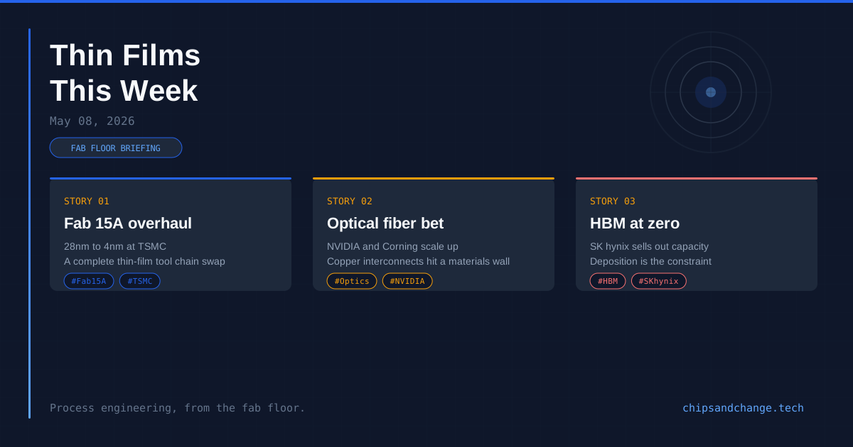
    1. TSMC Overhauls Fab 15A: 28nm → 4nm Means a Complete Thin-Film Tool Chain Swap

    What happened: TSMC has begun converting its Fab 15A in Central Taiwan Science Park from legacy 28/22nm production to 4nm-class manufacturing, with NT$100 billion (~$3.1B) in cleanroom and equipment investment. The company’s 1.4nm Taichung site is simultaneously coming together ahead of schedule.

    Thin films take:
    This isn’t a fab “retooling” — it’s a gut-and-rebuild. I’ve lived through node migrations before, and going from 28nm planar to FinFET-class 4nm (N4/N5 derivative) means every deposition chamber in the line gets swapped. The legacy 28nm line ran thick TEOS SiO₂, conventional SiN, and aluminum pad metallization — workhorse recipes on mature PECVD and PVD hardware. 4nm means cobalt interconnects, area-selective ALD for self-aligned vias, high-aspect-ratio gap-fill with cyclic deposition-etch processes, multi-layer EUV hardmask stacks, and low-k dielectrics that can’t survive a wet clean. That’s a full changeout of PECVD, PE-ALD, thermal ALD, and PVD chambers from every major tool vendor. Fab 15A’s old Applied Materials Producer and Lam Sequel chambers won’t see a single wafer at 4nm. The relocation of that legacy gear to secondary markets (mature-node fabs in China, foundry partners) is its own logistics story. Meanwhile, the 1.4nm Taichung greenfield coming together ahead of schedule suggests the tool install teams are pulling double shifts on both projects. For those of us in process integration, this means six months of intense qualification lots, film stress matching on new chamber hardware, and probably a few dozen OOC events before the deposition recipes converge.

    Key claim: Every single thin-film deposition chamber in Fab 15A is being replaced — 4nm uses fundamentally different dielectrics, liners, and metallization than 28nm.


    2. NVIDIA and Corning Bet Big on Optical Fiber — Copper Interconnects Face a Materials Challenge

    What happened: NVIDIA announced a multi-year partnership with Corning investing an initial $300M (scaling up to $3.2B) to build three new U.S. optical fiber plants, aiming to replace copper cabling in AI rack-scale systems with advanced optical connectivity.

    Thin films take:
    The copper-vs-optical debate in data center interconnects has been simmering for years, but this deal tells me the inflection point is real. From a thin-films perspective, optical fiber itself is a layered dielectric structure — the cladding and core are doped silica deposited by modified CVD (OVD or VAD processes, not PECVD but chemically analogous). What’s more interesting for our world is the coating stack: each fiber gets dual-layer UV-cured acrylate coatings for mechanical protection, applied on-draw at line speeds exceeding 50 m/s. The film thickness uniformity requirement (±2 µm on a 250 µm coating) is less demanding than wafer processing, but the throughput requirements are staggering. On the transceiver side — and this is where semiconductor thin films come back in — these fibers terminate in silicon photonics or InP PICs that demand precisely controlled dielectric cladding layers (SiO₂, SiN, oxynitride) deposited by PECVD on 300mm wafers, then integrated with copper BEOL stacks. NVIDIA’s bet is that the optical I/O energy-per-bit advantage justifies replacing miles of copper traces in DGX pods. For process engineers, this means more wafers running through photonic-specific PECVD and ALD processes, and growing demand for edge-coupling AR coatings and spot-size converters that require nanometer-precision deposited tapers.

    Key claim: Optical fiber is itself a precision thin-film structure (dual-layer UV-cured coatings on doped silica), and the transceiver ecosystem it feeds depends on PECVD-deposited dielectric cladding on 300mm photonic wafers.


    3. SK Hynix Hits Zero Available HBM Capacity — The Advanced Packaging Deposition Constraint Bites

    What happened: SK Hynix reports effectively zero available HBM3 and DRAM capacity, with customers (NVIDIA, Google, Amazon, Microsoft) offering to co-invest in new fab lines, buy EUV tools, and fund expansion just to secure allocation.

    Thin films take:
    People see “memory shortage” and think bit density — but anyone who’s spent time in a packaging fab knows the real bottleneck isn’t the front-end transistor. It’s the back-end-of-line and advanced packaging. HBM3E stacks 12 dies vertically, each connected by through-silicon vias (TSVs) that demand conformal SiO₂ liner deposition by PE-ALD at aspect ratios exceeding 20:1, a barrier/seed stack (TiN/Cu by PVD or ALD) with step coverage below 5% on the sidewall, and then bottom-up copper electroplating. Every TSV in every tier of every stack. Then there’s hybrid Cu-Cu bonding — the die-to-die interface requires CMP planarization of the Cu/dielectric surface to <1nm RRMS before plasma activation and room-temperature direct bonding. That’s a surface preparation and surface chemistry problem as much as a deposition one. If SK Hynix’s capacity is truly zero, it means their TSV etch/deposition and hybrid bonding lines are at 100% utilization — and the bottleneck becomes how quickly Lam, AMAT, and TEL can ship and install the next generation of TSV PE-ALD chambers and bonders (SUSS, Applied) into the new M15X and Yongin fabs. The customer offers to buy EUV machines are dramatic, but what they should be offering to fund are TSV dielectric ALD tools and Cu-Cu bonder platforms — the front-end lithography isn’t what’s constraining HBM output; the inter-die connectivity stack is.

    Key claim: SK Hynix’s HBM capacity crisis is fundamentally an advanced packaging deposition constraint — TSV dielectric ALD, Cu seed PVD, and hybrid bonding surface preparation are the real gating processes, not front-end lithography.


    That’s your Fab Floor Briefing for May 08, 2026. Next week we’ll be watching TSMC’s 1.4nm tool install roadmap, the Corning/NVIDIA fiber coating specs, and whether the SK Hynix customer co-investment model changes how deposition tool capacity is reserved.

  • The ‘Old’ Chip Crisis: Why 28 nm Still Rules the World

    The ‘Old’ Chip Crisis: Why 28 nm Still Rules the World

    # The “Old” Chip Crisis: Why 28 nm Still Rules the World

    Every headline about the semiconductor industry focuses on the bleeding edge — 3nm, 2nm, gate-all-around transistors, and AI accelerators. But the chips that actually run the world are made on nodes that are a decade old. The automotive in your car, the microcontroller in your medical device, the power management IC in your phone charger, the RF chip in your 5G base station — most of these are built on 28nm, 40nm, 65nm, or even 180nm processes.

    And here’s the uncomfortable truth: demand for these “old” nodes is exploding faster than supply can keep up.

    A TSMC 28nm wafer costs $3,000 — roughly one-sixth the price of a 3nm wafer (Silicon Analysts, 2026). But the more important number is this: the 28nm node generated more revenue for TSMC in 2024 than any of its older nodes, and demand hasn’t stopped climbing. Automotive electrification, IoT proliferation, industrial automation, and the buildout of 5G infrastructure are all driving a surge in mature-node demand that the industry’s foundry capacity wasn’t built to handle.

    The Node That Won’t Die

    The 28nm node entered production in 2011. It has now been in high-volume manufacturing for fifteen years — an eternity in an industry where the leading edge advances every 2-3 years. By the standards of silicon technology, 28nm should be ancient history.

    Instead, it’s more important than ever.

    Why 28nm has staying power:

    1. Cost. At $3,000 per wafer, 28nm is affordable for a massive range of applications. A simple IoT microcontroller on 28nm might cost $1-2. The same die on 3nm would cost 6-10x more for no real benefit, since the application doesn’t need the density or performance.

    2. Analog performance. Transistors at 28nm still have good analog characteristics — high breakdown voltage, low flicker noise, good matching. As you shrink below 28nm, analog performance degrades significantly. This is why mixed-signal chips, power management ICs, and RF circuits tend to stay on mature nodes. A 3nm transistor switches faster, but it can’t handle 5V signals or drive high currents.

    3. Design cost. As noted in our first article, designing a 28nm chip costs approximately $40 million versus $590 million at 3nm (IBS, 2025). For a company designing an automotive microcontroller that will sell for $15, those economics are decisive. You can’t amortize $590 million over a chip that makes $3 in profit per unit.

    4. Reliability. Mature nodes are incredibly well-characterized. 28nm has been qualified across hundreds of millions of device-hours. Automotive-grade 28nm processes meet AEC-Q100 requirements and support operating temperatures up to 150°C. Defense-grade processes meet MIL-STD requirements. The reliability data is thousands of pages thick. A new node would need 5-10 years to achieve similar qualification coverage.

    5. Established supply chain. The equipment set for 28nm is fully depreciated and well-understood. Fab engineers know every failure mode. The supply chain for materials, spares, and chemicals is optimized. When you’re running a 28nm fab, you’re not solving new problems — you’re optimizing throughput.

    Key fact: 28nm (and its derivative 22nm) is expected to account for approximately 15-20% of TSMC’s revenue through 2027 and beyond. The node has been in production for 15 years and shows no signs of decline. (TrendForce, 2025)

    The Capacity Crunch Nobody Talks About

    The 2021-2023 semiconductor shortage was widely covered as an automotive chip crisis. What was less understood: the crisis was almost entirely a mature-node crisis. The chips in short supply — microcontrollers, power management ICs, display drivers, sensors — were all on 28nm to 180nm processes. The leading-edge AI chips that hogged the headlines were actually in ample supply.

    The issue was capacity allocation. During the pandemic, automakers canceled chip orders, then tried to reinstate them when demand came roaring back. Foundries had reallocated that capacity to consumer electronics and other applications. And here’s the structural problem: you can’t quickly add mature-node capacity.

    Building a new 28nm fab costs $5-10 billion and takes 2-3 years. But more importantly, the equipment for 28nm is no longer in high-volume production. The lithography tools, deposition chambers, and etch systems that TSMC’s 28nm fabs use are based on older designs that ASML, Applied Materials, and Lam Research stopped manufacturing years ago. You can’t just order a new 300mm 28nm production line from a catalog. You’d need to source used equipment, commission it, and qualify it — a process that takes 12-18 months even with experienced teams.

    The result is a structural supply constraint. Global mature-node capacity (28nm and larger) is estimated at approximately 6-7 million wafer starts per month across all foundries. Demand is estimated at 7-8 million wafer starts per month and growing. The gap of 15-20% creates persistent shortages in automotive, industrial, and medical chips.

    Who Cares About 28nm? Everyone.

    Let me be specific about which industries are most affected by the mature-node crunch:

    Automotive is the biggest driver. A modern mid-range car contains 1,000-1,500 chips. Of those, maybe 10-20 are on advanced nodes (the infotainment SoC, the ADAS processor). The rest — powertrain controllers, body control modules, sensor interfaces, battery management ICs — are on 28nm to 180nm. The transition to electric vehicles actually increases the demand for mature-node chips, because EVs have more power management ICs, more sensor interfaces, and more motor controllers than ICE vehicles.

    Industrial automation and IoT are rapidly growing markets. An industrial sensor that runs for 5 years on a coin cell battery needs an ultra-low-power microcontroller, not a 3nm GPU. The LoRaWAN modem, the temperature sensor signal chain, the wireless MCU — all on mature nodes.

    Medical devices are almost entirely on mature nodes. A pacemaker, a hearing aid, a continuous glucose monitor, a defibrillator — none of these need leading-edge compute. They need ultra-low power consumption, high reliability, and small die area (but not microscopic transistors). Medical device qualification cycles are 3-5 years minimum, so once a design is locked to a node, it stays there.

    Defense and aerospace use mature nodes almost exclusively, for reliability reasons. The F-35’s electronic warfare system runs on 65nm and 45nm chips. Military-grade process qualification takes years, and the volumes are too low to justify leading-edge economics.

    The Economic Reality

    Here’s the tension that policymakers and investors don’t fully appreciate: the profit margins on mature-node chips are thinner, but the volumes are larger.

    A 3nm AI accelerator might sell for $15,000-30,000 (an NVIDIA H100-class part) with gross margins of 70-80%. But the total addressable market is maybe 10 million units per year across all vendors. A 28nm automotive microcontroller sells for $5-20 with gross margins of 40-50%. But the market is billions of units per year. The revenue opportunity in mature nodes, in aggregate, may actually be larger than the leading edge.

    This is why the CHIPS Act’s focus on leading-edge fabs — while strategically essential — may miss a key economic reality. The US and its allies don’t just need 3nm and 2nm fabs. They need 28nm, 40nm, and 65nm capacity. The current funding and incentives overwhelmingly favor leading-edge construction, but the supply bottleneck is at the mature end of the spectrum.

    An underappreciated risk: If mature-node capacity doesn’t expand, we’ll see recurring shortages in automotive and industrial chips — not because of another pandemic, but because demand structurally outpaces supply. The “everything shortage” of 2021-2023 wasn’t a one-off. It was a preview of the mature-node supply-demand imbalance that will persist through 2030.

    The Rise of the Specialty Foundries

    The mature-node market isn’t all TSMC. In fact, the landscape is more diverse than at the leading edge:

    • UMC (Taiwan) — Strong position in 28nm and 22nm, capacity expansion ongoing
    • GlobalFoundries (US) — Focused on 12nm-180nm for automotive, defense, and IoT. Public offerings have funded capacity expansion
    • SMIC (China) — Strong in 28nm-180nm for the domestic Chinese market. Under export restrictions for leading-edge tools
    • STMicroelectronics (Europe) — IDM with strong mature-node position in automotive and industrial
    • Texas Instruments (US) — Major investment in 300mm mature-node capacity in Texas and Utah
    • Renesas, NXP, Infineon — IDMs with captive mature-node fabs for automotive

    These specialty foundries and IDMs are investing billions in new capacity. GlobalFoundries is spending $4 billion to expand its Singapore and New York fabs. TI’s $30 billion investment in new 300mm fabs in Sherman, Texas is one of the largest single corporate investments in US manufacturing history — and it’s entirely for mature-node analog chips, not leading-edge digital.

    Key fact: Texas Instruments is investing $30 billion in new 300mm mature-node fabs in Sherman, Texas, focused on 28nm to 130nm analog and embedded processing chips. This is the largest single manufacturing investment focused entirely on mature nodes. (TI Investor Relations, 2024-2025)

    Can New Nodes Compete with 28nm?

    One counterargument: won’t the industry just migrate mature-node designs to newer, cheaper nodes over time? The answer is: not really, for a few reasons.

    28nm was the last planar node. At 28nm, transistors are still planar (laid flat on the silicon surface). Below 28nm, FinFET transistors (where the channel sticks up like a fin) become necessary for performance and leakage control. FinFETs are fundamentally different devices — different electrical characteristics, different design rules, different modeling. Migrating a 28nm design to 16nm FinFET requires a complete redesign, not a simple shrink.

    The “sweet spot” for cost is at 28nm. Even though 16nm wafers are denser, the per-wafer cost is significantly higher. For chips with moderate die area and high voltage requirements, 28nm often has the lowest total system cost.

    28nm has better off-state leakage. For battery-powered applications that spend most of their time in sleep mode, 28nm’s transistor characteristics are often superior to FinFET nodes. A 28nm microcontroller can draw nanowatts in sleep mode; a 16nm FinFET version might draw microamps. For a medical implant that needs to last 10 years, that difference is decisive.

    What This Means for the Industry

    The mature-node crunch has implications across the semiconductor value chain:

    For chip designers: Expect longer lead times and higher costs for 28nm tapeouts. Foundries are increasingly selective about which mature-node designs they accept, prioritizing high-volume, long-lifecycle applications (automotive, industrial) over lower-volume consumer designs. Designers should plan for 40-52 week lead times on mature-node wafers.

    For equipment companies: The market for used 300mm equipment has never been stronger. Companies that can refurbish and qualify older lithography, deposition, and etch tools for 28nm production have a significant market opportunity. Applied Materials and Lam Research have launched new programs to support “extended-life” mature-node equipment.

    For investors: The traditional semiconductor narrative — “newer is always better” — misses the reality that mature-node capacity is structurally undersupplied. Companies with strong mature-node positions (Texas Instruments, GlobalFoundries, STMicroelectronics) may offer more predictable growth than leading-edge companies with massive capex requirements.

    For policymakers: Mature-node capacity should be part of any comprehensive semiconductor strategy. The CHIPS Act’s R&D programs and manufacturing incentives should explicitly support new mature-node fabs, not just leading-edge. A car doesn’t run on 3nm chips — it runs on 28nm, 40nm, and 65nm chips. A secure semiconductor supply chain requires both.

    Conclusion

    The semiconductor industry has a bias toward the new and the shiny. The media covers the 3nm GPU launch, not the 28nm automotive MCU that ships 50 million units a year. But the chips that run the world aren’t the ones that make headlines. They’re the “old” chips on 28nm, 40nm, and 65nm — built on technologies that are a decade or more old, produced in volumes that dwarf the leading edge, and essential to every modern industry.

    The mature-node capacity crunch is the semiconductor industry’s hidden crisis. It doesn’t get the attention of AI or geopolitics, but it affects more industries and more people. And it’s not going away.

    The next time someone tells you the most important chip in the world is on 3nm, ask them what the sensor reading that data is running on. The answer is almost certainly 28nm.


    This article is part of the Fab Floor Reality pillar of Chips & Change. For the broader economic context, see our article on The Silicon Ceiling: Why ‘Change’ Is No Longer Optional.

    Frequently Asked Questions

    Why can’t they just make more 28nm chips?

    The equipment for 28nm fabs is no longer in volume production. New 300mm fabs for 28nm require sourcing used equipment, which is expensive and time-consuming. Additionally, foundries are prioritizing capital investment in leading-edge fabs where margins are higher.

    Is 28nm good enough for AI?

    For AI inference at the edge, sometimes — 28nm can run efficient inference for small models. For training or large language model inference, no. But AI training makes up a tiny fraction of the total semiconductor market by volume.

    Are newer nodes cheaper per chip?

    For very large, dense digital chips, yes. For analog-heavy, mixed-signal, or high-voltage chips, no. The per-transistor cost has flatlined since 28nm, and for many applications the total system cost favors mature nodes.

    Will we run out of mature chips again?

    Recurring shortages in specific mature-node segments are likely through 2028-2030 as demand growth outpaces capacity additions. The shortages won’t be as acute as 2021-2023 but will create persistent supply constraints in automotive and industrial markets.

  • Stress and Strain Engineering in Thin Films: What Every Process Engineer Should Know

    Stress and Strain Engineering in Thin Films: What Every Process Engineer Should Know

    If you’ve ever watched a wafer bow after deposition and wondered whether it’s the process or the substrate, you’re asking the right question. Residual stress in thin films is one of those problems that touches every deposition engineer’s work, whether you run PVD TiN barriers or CVD tungsten plugs. The stresses can be large enough to crack wafers, delaminate films, or shift transistor performance — and decoupling the causes is half the battle.

    Where Does Intrinsic Stress Come From in Sputtered Films?

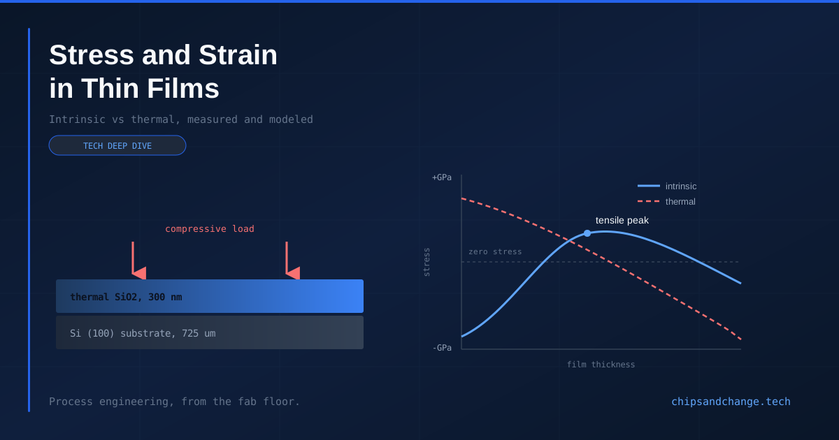
    The stress evolution in sputtered transition metal nitrides like TiN and TaN is a dynamic competition. On one side, you have atomic peening — energetic particles bombarding the growing film, driving atoms into interstitial sites and densifying the lattice. This generates compressive stress. On the other side, microstructural relaxation and shadowing at higher pressures creates porous, columnar microstructures that pull together and generate tensile stress (Windischmann, 1991).

    The key parameter is particle kinetic energy. At low deposition pressures and high substrate bias, sputtered atoms and reflected neutrals hit the surface with enough energy to “peen” it, forcing atoms into non-equilibrium positions. Manova et al. (2010) showed this creates a lateral expansion force that, constrained by the substrate, manifests as macroscopic compressive stress. Crank up the pressure, and gas-phase collisions thermalize the flux. You get oblique incidence, shadowing, and a shift toward tensile stress — the classic Zone 1 of the Thornton model.

    The practical takeaway: if you’re seeing unexpected wafer bow, check your pressure and bias before you touch the chemistry.

    How Do You Decouple Thermal Stress from Intrinsic Stress?

    This is where the metrology gets interesting. Thermal stress comes from CTE mismatch between film and substrate — heat the film, it wants to expand at a different rate than the silicon below it. Intrinsic stress comes from the growth process itself.

    The standard decoupling method is temperature-dependent stress measurement using the Stoney equation or XRD. Here’s how it works:

    1. Deposit the film and measure the as-deposited curvature

    2. Heat the sample and track the stress-temperature slope (dσ/dT)

    3. The slope gives you the pure thermal (CTE) component

    4. The intercept at deposition temperature gives you the intrinsic stress

    Researchers also use X-ray diffraction — comparing the as-deposited lattice strain to a relaxed reference lets you separate microstructural from thermal strain directly (Abadias et al., 2019). And there’s a clever variable-substrate approach: deposit the same film on silicon and sapphire simultaneously. Since intrinsic stress depends on the growth process, not the substrate, the difference in total measured stress lets you solve for both the intrinsic component and the film’s CTE.

    Beyond Graded Buffers: Strategies for III-V on Silicon

    Managing strain at the film-substrate interface becomes even more critical when you’re growing III-V materials on silicon. The lattice mismatch produces threading dislocation densities (TDD) that can kill device performance.

    Beyond the standard toolbox of graded buffers and compliant substrates, several strategies have emerged:

    Aspect Ratio Trapping (ART): Grow the III-V material inside high-aspect-ratio trenches etched into a dielectric. Dislocations propagate at specific crystallographic angles (54.7° for {111} planes in zinc-blende), so they terminate at the sidewalls instead of reaching the active layer.

    Dislocation Filter Layers (DFLs): Thin, strained-layer superlattices (like InGaAs/GaAs) whose alternating strain fields bend threading dislocations laterally, increasing the chance that two dislocations meet and annihilate.

    Quantum Dot Filters: Self-assembled InAs/GaAs quantum dots create localized 3D strain fields that are significantly more effective at pinning dislocations than planar superlattices. This has enabled lasers on silicon with TDD in the 10⁶ cm⁻² range — orders of magnitude lower than conventional heteroepitaxy.

    Non-equilibrium deposition routes offer kinetic handles that MBE and MOCVD don’t. Pulsed laser deposition (PLD) delivers species with 10-100 eV kinetic energy, enhancing surface mobility even at low substrate temperatures and suppressing islanding in high-strain systems. Migration Enhanced Epitaxy (MEE) alternates group III and group V pulses, preventing the formation of surface dimers that restrict adatom migration, allowing high-quality interfaces at significantly lower temperatures.

    The Engineer’s Bottom Line

    For process engineers running deposition tools, the lesson is straightforward: residual stress isn’t a black box. It’s a competition between particle energy and microstructure, and you can diagnose it systematically with thermal cycling and XRD. The trend in advanced integration — from ART trenches to QD filters — shows that the industry is getting better at managing strain at the atomic level. But the fundamentals of peening, shadowing, and CTE mismatch aren’t going anywhere.

    Frequently Asked Questions

    What’s the simplest diagnostic for stress in thin films?

    Wafer curvature measurement using the Stoney equation. Run it before and after deposition, and if possible, through a thermal cycle to separate intrinsic from thermal components.

    Can you have both compressive and tensile stress in the same film?

    Yes — stress can vary through the film thickness. The top surface might be compressive from ion bombardment while the bottom layers are tensile from columnar growth. This is why stress-thickness product (not just stress) is the relevant metric for process control.

    Is substrate bias always beneficial for stress control?

    Not necessarily. While bias increases ion energy and can drive compressive stress, excessive bias can cause resputtering, argon entrapment, and damage to sensitive device layers. The optimal bias depends on your film thickness and device architecture.

  • The Geopolitics of the Angstrom: Fabs as the New Oil Fields

    The Geopolitics of the Angstrom: Fabs as the New Oil Fields

    # The Geopolitics of the Angstrom: Fabs as the New Oil Fields

    In the 20th century, nations competed for oil fields. In the 21st, they compete for fabs.

    The semiconductor fab has become the single most strategically valuable piece of industrial infrastructure in the world. Not because it produces chips — but because the country that controls leading-edge chip manufacturing controls the flow of compute power that underpins AI, military systems, financial infrastructure, and every advanced technology industry.

    The numbers are staggering. TSMC alone controls roughly 90% of the global market for sub-7nm chip manufacturing. A single Taiwanese company decides whether NVIDIA can ship Blackwell GPUs, whether Apple can launch new iPhones, and whether AMD’s MI300X accelerators can reach data centers. This concentration of capability in one geographic region, on an island 180 kilometers from mainland China, is widely described as the greatest concentration of strategic risk in the global supply chain.

    In response, the United States has committed $53 billion through the CHIPS and Science Act of 2022. The European Union is investing €43 billion through its European Chips Act. Japan, South Korea, India — every major economy is launching semiconductor subsidy programs. Global government investment in semiconductor manufacturing capacity has exceeded $200 billion in announced subsidies since 2020 (SIA, 2025).

    This isn’t industrial policy as usual. This is the semiconductor equivalent of a global arms race.

    The Taiwan Conundrum

    Before the geopolitics, the geography: Taiwan produces over 60% of the world’s semiconductor output by revenue, and an estimated 90% of advanced chips (7nm and below) are manufactured in Taiwan at TSMC (and a smaller share at UMC). TSMC itself is the world’s most important company most people have never thought about.

    The stakes are straightforward: If TSMC’s fabs were disrupted — whether by military action, earthquake, or blockade — the global technology economy would stop. Not slow down. Stop. AI training would halt. Smartphone production would collapse. Advanced military systems would lose their compute backbone.

    This is not a theoretical risk. Taiwan sits on the Pacific Ring of Fire and experiences frequent earthquakes. More significantly, the People’s Liberation Army has made increasingly explicit statements about Taiwan’s status, and the island’s semiconductor manufacturing dominance is a central concern. Taiwan’s “silicon shield” — the theory that TSMC’s strategic importance protects the island from invasion — works both ways. It keeps Taiwan safe, but it also makes the global economy dangerously dependent on a single country for its most critical technology.

    Key statistic: Taiwan Semiconductor Manufacturing Company (TSMC) manufactures approximately 90% of the world’s most advanced chips (sub-7nm). Its two main 3nm fabs are located in Tainan and Taichung — both less than 200 km from the Chinese coast. (SIA Report on Semiconductor Supply Chain, 2025)

    The Chips Act Reality Check

    The US CHIPS and Science Act authorized $53 billion — $39 billion for manufacturing incentives and $11 billion for R&D — with the explicit goal of reshoring leading-edge semiconductor production. Two years in, the results are mixed.

    What’s been awarded: Major grants have gone to Intel, Samsung, TSMC, Micron, and GlobalFoundries for fab construction in Arizona, Texas, Ohio, New York, and Idaho. TSMC’s Arizona fab — initially announced at $12 billion and escalated to $65 billion across three phases — began production of 4nm chips in late 2025. Intel’s Ohio “megafab” and Samsung’s Texas expansion are under construction with multi-billion dollar government support.

    What’s been disbursed: Here’s the gap. As of early 2026, only a fraction of the announced awards have been turned into actual cash disbursements. The Department of Commerce has been conservative in releasing funds, using preliminary memoranda of terms (PMTs) that require milestone achievement before money flows. This “money before, then more money later” structure creates tension between construction timelines and government oversight.

    What’s often missed: The CHIPS Act is not just about the $53 billion. It’s also about the investment tax credit (Section 48D of the Internal Revenue Code) that provides a 25% credit for semiconductor manufacturing investments. This backstop is worth an estimated $50-80 billion over the next decade — and doesn’t require government appropriations.

    The real challenge isn’t money. It’s people. Building a state-of-the-art fab requires thousands of specialized engineers — process engineers, facilities engineers, equipment maintenance technicians — that the US workforce doesn’t have in sufficient supply. TSMC’s Arizona project has faced repeated delays partly because experienced Taiwanese engineers need to train local teams. The company has flown in hundreds of Taiwanese engineers to Arizona to accelerate the ramp, which has created local friction and highlighted the talent gap.

    Europe and Japan Make Their Moves

    The European Chips Act (€43 billion) aims to double Europe’s global market share from 10% to 20% by 2030. Intel has committed to building a massive fab complex in Magdeburg, Germany, expected to cost €30 billion. TSMC is building a €10 billion specialty fab in Dresden with Bosch, Infineon, and NXP as partners.

    Japan, leveraging the Rapidus initiative and government subsidies of nearly ¥4 trillion ($27 billion), is attempting to leapfrog to 2nm production by 2027 — an audacious goal for a country that currently has no leading-edge manufacturing. The strategy pairs Japanese equipment expertise (Tokyo Electron, Screen Semiconductor Solutions) with IBM’s 2nm design IP and, reportedly, support from Imec.

    South Korea has its K-Semiconductor Strategy with tax credits and infrastructure support for Samsung and SK Hynix. Samsung is building its $17 billion Taylor, Texas fab to complement its existing Austin facility.

    Key statistic: Global announced government subsidies for semiconductor manufacturing exceed $200 billion as of 2025, per SIA tracking. Actual disbursement lags significantly behind announcements. (SIA, 2025)

    The China Containment Strategy

    The other pillar of semiconductor geopolitics is export control. Beginning in October 2022, the US Commerce Department imposed increasingly stringent controls on the export of advanced semiconductor equipment, EDA software, and certain AI chips to China.

    The objective: Prevent China from acquiring the tools and technology needed to develop indigenous leading-edge chip manufacturing capability. If China cannot buy EUV lithography tools from ASML, cannot access certain deposition and etch tools from US suppliers, and cannot use EDA tools from Synopsys and Cadence, then China’s foundries (SMIC, Hua Hong) cannot produce competitive 5nm or 3nm chips.

    The effect so far: China has responded by accelerating its own equipment development. SMIC has managed to produce 7nm-class chips using DUV lithography with multi-patterning — a technically impressive but economically painful workaround. Yield is low and cost is high. China’s domestic equipment ecosystem is growing but remains several generations behind ASML, Tokyo Electron, and Applied Materials.

    The unintended consequence: Export controls have also hurt US equipment companies. Applied Materials, Lam Research, and KLA have lost significant China revenue (approximately 15-25% of total sales). The controls create a wedge between the US equipment industry’s business interests and US national security objectives.

    The second-order effect China cares about: Huawei’s Kirin 9000S processor, fabricated by SMIC on a 7nm-class process and discovered in the Mate 60 Pro in 2023, demonstrated that China can produce competitive chips under sanctions. The performance-per-watt gap between SMIC’s 7nm and TSMC’s 3nm is enormous, but the existence of a domestic alternative changes the strategic calculus.

    The Talent War

    The most underappreciated dimension of semiconductor geopolitics is human.

    The semiconductor workforce is aging. In the US, the average semiconductor industry worker is over 45. Fewer students are pursuing semiconductor engineering degrees relative to software engineering. The industry faces a projected shortage of 70,000-90,000 workers over the next five years (SIA / Oxford Economics, 2024).

    Taiwan’s advantage isn’t just TSMC’s tools — it’s TSMC’s people. The company has 70,000+ employees who have spent their entire careers in advanced semiconductor manufacturing. The tacit knowledge — the stuff that can’t be written down in process recipes but lives in engineers’ intuitions — is irreplaceable. This is why TSMC’s Arizona ramp has been slower than expected. You can’t train a decade of experience in twelve months.

    Materials science talent is the bottleneck within the bottleneck. Every new fab needs process engineers who understand deposition, etch, lithography, and metrology at a deep level. The US produces roughly 1,200 materials science and engineering PhDs per year. China produces about 5,000. The talent pipeline is structurally imbalanced, and the industry hasn’t invested enough in university partnerships, apprenticeship programs, or workforce development to close the gap.

    What a Decoupled World Looks Like

    If the trend continues — US/EU/Japan reshoring on one side, China building autonomous capability on the other — the semiconductor industry will look very different in 2030.

    Scenario A: Managed decoupling (most likely). Two parallel semiconductor ecosystems emerge. The US-led ecosystem (TSMC Arizona, Intel, Samsung Texas, GlobalFoundries) produces leading-edge chips for the West. The Chinese ecosystem (SMIC, Hua Hong, domestic equipment) produces adequate-but-behind chips for itself and allied markets. The cost premium for “secure” chips is 15-30%, absorbed by governments and strategic customers.

    Scenario B: Taiwan disruption (low probability, catastrophic impact). A military or natural disaster disrupts TSMC’s Taiwan operations for six months or more. Global chip supply contracts by 40-60% at the leading edge. AI development stalls. Smartphone and data center prices surge. The US strategic semiconductor reserve — if it exists — proves insufficient.

    Scenario C: Technology leapfrog (unlikely but possible). A new transistor architecture, beyond-GAA technology, or a photonics breakthrough renders current fab investments partially obsolete. The country that commercializes this technology first resets the competitive landscape.

    What It Means for the Fab Floor

    I want to close with a perspective that strategic analysts often miss because they’ve never stood in a cleanroom.

    The geopolitics of chips is discussed in terms of billions of dollars, national security strategy, and trade policy. But on the fab floor, it’s about process control, mean time between failure, and whether the deposition chamber can hold 0.1% uniformity across a 300mm wafer. The gap between what governments announce and what fabs can actually deliver is enormous, and it’s measured in angstroms.

    A fab is not a factory in the traditional sense. It’s a building that costs $20 billion, takes 3-5 years to construct, runs 24/7 for decades, and requires a specialized workforce that takes years to develop. You can’t “reshore” a semiconductor supply chain with press releases. You reshore it one process step, one engineer, and one qualified material at a time.

    The CHIPS Act money is real. The fab construction is happening. But the industry should be honest about timelines. The $53 billion buys the beginning of a reshored supply chain — not the end of one. The semiconductor industry operates on decade-long cycles, and the geopolitical competition to control it will be the defining industrial story of the 2020s and 2030s.


    This article is part of the Geopolitics & Markets pillar of Chips & Change. For an analysis of the domestic economics that make semiconductor reshoring so difficult, see our piece on 28nm and the Mature Node Market.

    Frequently Asked Questions

    Why is TSMC so dominant in advanced chips?

    TSMC has accumulated 30+ years of manufacturing experience, invests $30-40 billion annually in capex, and serves every major chip designer (Apple, NVIDIA, AMD, Qualcomm) without competing with them in chip design. This “pure-play foundry” model gives it unmatched scale and neutrality.

    Can the US become self-sufficient in chip manufacturing?

    Not in the short term. Even with the CHIPS Act and Intel’s investment, the US will need imported materials, equipment, and some specialized expertise for at least 5-10 years. Full self-sufficiency is probably not the goal — supply chain resilience with trusted partners is.

    How much of the CHIPS Act has been spent?

    As of early 2026, the Department of Commerce has announced multiple preliminary agreements but has disbursed a relatively small percentage. Most grants use milestone-based disbursement, with final payment tied to production milestones.

    Will China catch up to TSMC?

    China faces a 5-7 year technology gap at the leading edge and is constrained by export controls on EUV lithography equipment. But its domestic equipment ecosystem is developing rapidly. A breakout — a Chinese company producing competitive 5nm or 3nm chips by 2030 — cannot be ruled out.

  • Thin Films This Week — May 1, 2026

    Thin Films This Week — May 1, 2026

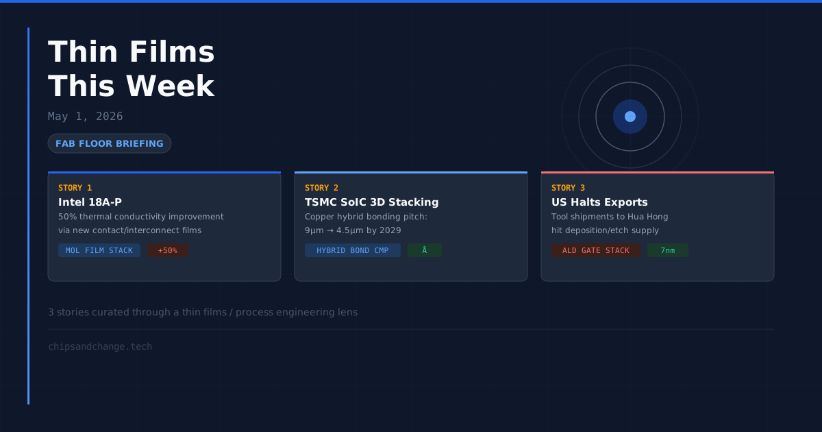
    Story 1: Intel Details 18A-P — 50% Thermal Conductivity Improvement Via New Contact and Interconnect Films

    📰 What happened: Intel published a paper at VLSI 2026 detailing its 18A-P process node, introducing new high-performance and low-power RibbonFET variants with enhanced contacts, a 9% iso-power performance gain, and a 50% improvement in thermal conductivity.

    🔬 Thin films take: This 50% thermal conductivity number jumps off the page for anyone who’s spent time on a deposition tool. You don’t get that kind of improvement without fundamentally rethinking your contact and middle-of-line (MOL) film stack. The key enabler is almost certainly a new contact metal or liner — think cobalt or ruthenium replacing traditional tungsten in the contact plug, combined with a thinner, higher-quality TiN or TiAl barrier. GAA nanosheets already run hot because the channel is wrapped on all four sides by gate metal — there’s no bulky substrate to sink heat through the way planar FinFETs did. So Intel’s thermal play is about lowering the interfacial thermal resistance between the source/drain epitaxy and the contact metal. That means tighter process control on the silicide formation (likely TiSi or NiPtSi at these dimensions) and a smoother, cleaner interface with fewer phonon-scattering defects. The 18% power reduction at iso-performance also tells me they’ve optimized the high-k/metal gate stack — probably a thinner HfO2-based dielectric with a new capping layer to reduce gate leakage without sacrificing electrostatic control.

    One key claim: Intel’s 50% thermal conductivity improvement on 18A-P points to a complete overhaul of the MOL contact film stack — likely cobalt or ruthenium contacts with optimized silicidation — which cuts interfacial thermal resistance where GAA nanosheets need it most.

    Source: Tom’s Hardware — Intel details 18A-P

    Story 2: TSMC SoIC Roadmap Scales Hybrid Copper Bonding From 9µm to 4.5µm Pitch by 2029

    📰 What happened: TSMC outlined its SoIC 3D stacking roadmap with copper hybrid bonding pitch scaling from 9µm to 6µm (current generation) targeting 4.5µm by 2029, while accelerating TSV availability for A14 to just one year after initial production.

    🔬 Thin films take: The hybrid copper bonding pitch — 9µm → 6µm → 4.5µm — is a deposition and CMP problem as much as it is a lithography one. At these dimensions, the Cu-CMP step before bonding determines everything. You need mirror-smooth surfaces with angstrom-level dishing control across the full wafer, because any topography at the bonding interface creates voids that kill the dielectric seal and compromise electromigration lifetime. The dielectric layer — typically SiO₂ deposited by PECVD or PE-ALD — has to be dense enough to form a hermetic bond at sub-400°C temperatures required to protect underlying devices. TSMC’s ability to accelerate A14 TSV availability to just one year after node launch tells me they’ve solved a significant via-middle TSV integration issue — probably a new liner/barrier scheme that can handle the aspect ratios required for A14’s backside power delivery network. The film stress management challenge of stacking two thinned wafers with BSPDN on one side and hybrid bonds on the other is a multi-film stress engineering problem our simulation tools are still catching up to.

    One key claim: Scaling SoIC hybrid copper bonding to 4.5µm pitch by 2029 requires sub-angstrom CMP dishing control on the Cu/dielectric interface — a thin films process challenge that is harder than the lithography at these dimensions.

    Source: Tom’s Hardware — TSMC SoIC roadmap

    Story 3: US Halts Tool Exports to Hua Hong — Deposition and Etch Equipment Supply Chain Impacted

    📰 What happened: The US Commerce Department ordered chip equipment companies to halt shipments to Hua Hong Semiconductor and Huali Microelectronics, which are reportedly preparing a 7nm fab in Shanghai. Applied Materials and Lam Research stocks declined on the news.

    🔬 Thin films take: This one hits closer to home for anyone working deposition and etch. Hua Hong is primarily a specialty foundry running mature nodes for power management ICs, MCUs, and display drivers — heavy consumers of thick-film deposition processes (TEOS oxides, PSG/BPSG interlayer dielectrics, thick aluminum reflow for power devices). Cutting off tool access for specialty business is one thing, but the real story is the reported 7nm fab ambition. At 7nm, you need ALD high-k/metal gate stacks (HfO₂ with LaO or Al₂O₃ capping layers), advanced spacer films (Si₃N₄, SiBCN), and multi-layer EUV-compatible hardmasks. None of that is available from domestic Chinese tool makers at volume production scale. Naura has made progress on PVD and etch, and AMEC has dielectric etch tools that work, but ALD high-k deposition for a 7nm gate stack? They’re years behind Applied’s Centura and Lam’s Vector platforms. The cost here is measured in yield — every wafer that fails due to film thickness non-uniformity or particle contamination from a less mature tool is a direct hit. For specialty films like stress-engineered SiN liners that drive SRAM performance at advanced nodes, the process window is so tight that even mature tools struggle.

    One key claim: China’s domestic tool ecosystem lacks production-capable ALD platforms for 7nm high-k/metal gate stacks — Applied Materials and Lam Research control the film quality and uniformity that 7nm yield depends on.

    Source: Tom’s Hardware — US halts exports to Hua Hong; Reuters

  • The Silicon Ceiling: Why ‘Change’ Is No Longer Optional

    The Silicon Ceiling: Why ‘Change’ Is No Longer Optional

    # The Silicon Ceiling: Why “Change” Is No Longer Optional

    For fifty years, the semiconductor industry operated on a simple promise: make the transistors smaller, and everything else takes care of itself. That promise is broken. The physics still works — barely — but the economics stopped making sense somewhere between the 7nm and 3nm nodes. The industry that gave us Moore’s Law has hit a ceiling, and it’s not a physical one. It’s a financial one.

    Designing a chip at 5nm costs $416 million. At 3nm, that number jumps past $590 million (International Business Strategies (IBS), 2025). A single TSMC 3nm wafer now runs $19,500 — more than six times the cost of a 28nm wafer (Silicon Analysts, April 2026). Meanwhile, the transistor density gain from N5 to N3 was roughly 1.6x — significantly less than the 2x the industry spent decades expecting. Each node shrink delivers diminishing returns at exponentially rising costs.

    This isn’t the end of progress. It’s the end of one kind of progress — and the beginning of another. The semiconductor industry is entering an era where change no longer means “make it smaller.” It means architecture, packaging, materials, and integration. And for the companies and countries that recognize this, the opportunity is immense.

    How Did We Get Here? The End of the Free Lunch

    For decades, Dennard scaling gave the industry a near-free performance boost with each node. Smaller transistors meant faster, more power-efficient chips. You didn’t need clever architecture — the process node did the work.

    Dennard scaling broke around 2006, when leakage current made it impossible to keep power density constant. The industry compensated with multicore architectures. Then multicore hit the memory wall. Then the utilization wall. And the fixes got harder.

    By 2018, a single leading-edge fab cost $15-20 billion to build — roughly the GDP of a small country. TSMC’s upcoming 2nm fab in Arizona reportedly carries a $65 billion price tag across multiple phases. The capital intensity of the industry has inverted. It no longer costs less to do more.

    Key Fact: The design cost for a 28nm chip is $40 million. For a 7nm chip, it’s $217 million. For 5nm, $416 million. At 3nm, $590 million. And 2nm will likely cross $1 billion per design. (IBS, 2025)

    Only a handful of companies in the world can afford these numbers. Apple, NVIDIA, AMD, Qualcomm — maybe two or three others. Everyone else is locked out of the leading edge. This isn’t a healthy industry structure. It’s a bottleneck that throttles innovation across the entire technology stack.

    The Numbers Don’t Lie: The Cost Crisis at the Leading Edge

    Let me put some real numbers on this from a process engineer’s perspective.

    Wafer costs tell the story. A TSMC 3nm wafer costs $19,500 in 2026. At 5nm, it’s $18,500 — nearly the same price for a node that’s two generations old. At 7nm, it’s $9,500. At 28nm, it’s just $3,000 (Silicon Analysts, 2026). The gap between mature and leading-edge nodes isn’t linear — it’s exponential.

    But the wafer is only the beginning. Advanced packaging costs are now a major line item. TSMC’s CoWoS interposer packaging — required for any AI accelerator that integrates HBM memory — costs $70 per unit. The lead time is 40-52 weeks, and demand exceeds supply by 40-50%. A single H100-class GPU requires $300+ worth of HBM memory stacks plus packaging, pushing the total manufacturing cost past $3,300 per chip.

    The per-transistor cost, which declined for decades, has essentially flatlined since 28nm. We’re spending more per wafer to put transistors on it, but those transistors cost about the same as they did five years ago. The economic engine of Moore’s Law — cheaper transistors every generation — has stalled.

    Why “Smaller” Isn’t the Answer Anymore

    Here’s what the node names don’t tell you: a “3nm” transistor today is not 3 nanometers. The naming has become marketing. TSMC’s N3 process doesn’t have a 3nm gate length — it’s a branding term that correlates roughly to transistor density. The node names used to map to physical dimensions. Now they map to foundry marketing departments.

    The real metrics — density, power, and performance — tell a more honest story:

  • N5 to N3 — Approximately 1.6x logic density gain (TSMC claims 1.6x, real-world benchmarks show closer to 1.3-1.4x)
  • N7 to N5 — Roughly 1.8x density improvement
  • N10 to N7 — Approximately 1.6x
  • Compare this to the golden era: N28 to N20 delivered about 2x density. N20 to N16, another 2x. The consistent doubling that defined Moore’s Law for decades has degraded to 60-80% gains per generation. And each of those gains costs more than the one before.

    Meanwhile, 5nm wafer costs are nearly identical to 3nm. The foundry isn’t passing along cost savings — it can’t. EUV lithography tools cost $200 million each and consume more power than a small factory. A single EUV tool can process roughly 150-200 wafers per hour in high-volume manufacturing. The depreciation alone on those machines adds thousands of dollars to every wafer.

    Cracks in the System: What $590 Million Design Costs Mean

    The $590 million figure for a 3nm chip design isn’t just a number — it’s a structural barrier to entry. Here’s what it means in practice:

    You need to sell millions of units to break even. A company designing a custom 3nm chip needs to amortize that $590 million across every chip they sell. If the die cost per chip is $87 (for a 200mm² die at 3nm), and you add packaging, test, and margin, you’re at $100-150 per chip before you ship a single unit. Recouping $590 million in NRE means selling 4-6 million units at a $100 premium.

    Very few applications outside smartphones and data center AI can justify those volumes. Automotive? Maybe for premium ADAS chips. IoT? Forget it. Edge AI? Only the highest-end parts.

    This creates what I call the “silicon ceiling”: a market where only the biggest players play, and everyone else is stuck at 28nm, 40nm, or older nodes. The result is a bifurcated industry — bleeding-edge AI accelerators on one side, mature-node microcontrollers on the other, and very little in between. The mid-range has been hollowed out.

    The “Change” That’s Already Happening

    The interesting thing is that the industry has already figured this out. The response isn’t more transistor shrinks — it’s heterogeneous integration, chiplet architectures, and materials innovation. This is the “Change” in the title, and it’s already reshaping how chips are designed and built.

    Chiplets and UCIe

    Instead of building one massive monolithic die (expensive, low yield), companies are disaggregating designs into smaller chiplets fabricated on the optimal node for each function. An I/O die? 28nm or 16nm, where transistors are cheap and voltage handling is easy. A compute die? 3nm, where density matters. Memory? Stack it vertically.

    The Universal Chiplet Interconnect Express (UCIe) standard has gained remarkable traction since its launch in 2022. What started as an Intel-led initiative now counts AMD, Arm, Google, Meta, Microsoft, Qualcomm, Samsung, and TSMC as members. The standard provides the physical layer, protocol, and compliance framework for mixing and matching chiplets from different vendors on different nodes.

    This is the single most important architectural shift since the adoption of multicore processors. Chiplets break the $590 million barrier by letting you design only the bleeding-edge portion of your chip at 3nm, while putting the rest on cheaper nodes.

    Advanced Packaging as the New Front

    If chiplets are the what, advanced packaging is the how. The packaging line used to be an afterthought — a $0.80 QFN package for simple chips, maybe $8 for a flip-chip BGA. Today, packaging is a strategic bottleneck.

    TSMC’s CoWoS (Chip-on-Wafer-on-Substrate) capacity can’t keep up with demand. NVIDIA, AMD, and anyone building AI accelerators is competing for a limited supply of interposer capacity. CoWoS lead times of 40-52 weeks mean that the packaging line, not the fab, is the gating factor for AI chip supply.

    Intel’s EMIB and Foveros technologies represent a competing approach, using embedded bridges instead of full silicon interposers. AMD’s chiplet designs have been shipping for years, with the Ryzen and EPYC lineups using multiple 5nm and 6nm chiplets connected via Infinity Fabric on a silicon interposer.

    The advanced packaging market was valued at approximately $35-40 billion in 2025 and is projected to reach $60+ billion by 2030 (Yole Group, 2025). For context, that’s larger than the entire semiconductor capital equipment market was in 2010.

    Materials Innovation: Where the Real Work Happens

    This is where my perspective as a process engineer matters most. The headlines go to EUV lithography and gate-all-around transistors. But the real innovation — the stuff that determines whether a process actually works in high-volume manufacturing — happens in the materials stack.

    For LPCVD and thin film deposition — my world — the challenges are immense. Every new node adds layers: more metal layers for interconnect, more dielectric layers for isolation, more hard mask layers for patterning. A 3nm chip might have 15+ metal layers, each requiring precisely controlled film deposition.

    The materials requirements are changing in three critical ways:

    1. New dielectrics with lower k-values — needed to reduce RC delay in increasingly dense interconnect stacks. The industry is running out of materials that have both the right dielectric constant and the mechanical/thermal stability for manufacturing.

    2. Novel metal fill for interconnects — Cobalt and ruthenium are replacing copper in the most critical layers because they allow better gap fill at narrow dimensions. This isn’t a minor substitution; it requires entirely new deposition chemistries and process recipes.

    3. Sacrificial layers and selective removal — Gate-all-around (GAA) nanosheet transistors require selective epitaxial growth and precisely controlled etch stop layers. The process complexity for GAA is 2-3x that of FinFET.

    Every materials change requires months of process qualification. You can’t just order a new precursor from a chemical supplier and drop it into the fab. The qualification cycle — material selection, deposition characterization, electrical testing, reliability stress, yield ramp — takes 12-18 months minimum. This is the “valley of death” for materials startups, and it’s not getting easier.

    The bottom line: Materials innovation is the limiting factor for Moore’s Law continuation, not lithography. We can print transistors smaller than ever. What we can’t always do is build them out of materials that actually work in high-volume manufacturing.

    What This Means for the Industry

    The silicon ceiling has profound implications for how the industry operates:

    Fewer leading-edge players. We’ll see consolidation at the leading edge — fewer companies designing 3nm and 2nm chips. This isn’t necessarily bad; it’s an economic reality. But it means the center of gravity for semiconductor innovation shifts from “better transistors” to “better systems.”

    Growth in the “good enough” node market. The 28nm and 16nm nodes will remain viable for years. Automotive, industrial, IoT, and defense applications don’t need 3nm density. They need reliability, voltage handling, and affordable unit costs. These mature nodes will be the growth engine for companies like STMicroelectronics, NXP, and Renesas.

    The packaging line is now a first-class citizen. The companies that control advanced packaging capacity — TSMC, Intel, Samsung, and ASE — will have strategic leverage comparable to the foundries themselves. Expect massive capital investment in CoWoS, SoIC, and 3D packaging capacity over the next five years.

    Materials companies get a new lease on life. The shift to GAA transistors, new interconnects, and complex dielectric stacks means more materials innovation, not less. Applied Materials, Lam Research, and Tokyo Electron will see growing demand for deposition and etch tools that can handle new materials. But the qualification timeline remains the bottleneck.

    The Case for Optimism

    This sounds like a grim picture, but I don’t think it is. The silicon ceiling is a forcing function — it’s pushing the industry toward structural innovation that has been overdue for two decades.

    The shift from monolithic dies to chiplets is architecturally healthier. It allows design teams to use the right node for each function, rather than being forced onto an expensive bleeding-edge process that’s overkill for most of the chip.

    The rise of advanced packaging creates new differentiation vectors. When everyone has access to the same foundry nodes (they do — TSMC sells to everyone), the packaging integration becomes a competitive advantage. This is why NVIDIA’s lead isn’t just about GPU compute — it’s about CoWoS capacity and HBM integration expertise.

    Materials innovation becomes higher-value. When process shrinks delivered all the gains, materials scientists were supporting cast. In the chiplet-and-packaging era, materials choices — what goes into the interposer, how the microbumps are formed, the dielectric between stacked dies — are first-order design decisions.

    And for engineers who understand these systems holistically — process, packaging, architecture, economics — the career opportunity has never been better. The era of “just shrink it” required specialists. The era of “change” requires people who understand the full stack.

    Conclusion

    The semiconductor industry is hitting the silicon ceiling. The $590 million 3nm design cost, the $19,500 wafer, the 1.6x density gain — these aren’t temporary hiccups. They’re structural features of an industry that has reached the economic limits of transistor scaling.

    But the industry doesn’t end at the ceiling. It changes direction. The most exciting developments in semiconductors today aren’t about smaller transistors. They’re about smarter architecture (chiplets), more sophisticated integration (advanced packaging), and deeper materials science. The phrase “Chips & Change” isn’t a slogan — it’s a description of what the next decade of semiconductor innovation will look like.

    Change is no longer optional. It’s the only path forward. And for those ready to embrace it, the opportunity is enormous.


    This article is the first in an ongoing series from a semiconductor process engineer with a decade of experience in thin film deposition. For a deeper look at chiplets and heterogeneous integration, see future coverage on this topic.

    Frequently Asked Questions

    Is Moore’s Law dead?

    Not exactly — but the version of Moore’s Law that gave the industry free performance gains every 18-24 months is economically unsustainable. The industry is shifting from transistor scaling to system-level scaling through chiplets, packaging, and architecture.

    Why do 3nm chips cost so much to design?

    The $590 million figure includes mask costs ($15-20 million for a full mask set at 3nm), design tool licenses, verification, and engineering resources. The complexity of designing at 3nm — with hundreds of design rules, multi-patterning, and complex power grids — requires massive engineering teams working for 2-3 years.

    Will chip prices keep rising?

    Unit costs for leading-edge chips will likely rise, but system-level costs may stay flat or decrease as chiplet architectures allow mixing expensive compute dies with cheaper support dies. The “cost per function” can continue declining even if “cost per transistor” doesn’t.

    What is the most important technology for the next five years?

    Advanced packaging. The ability to integrate chiplets from different nodes, stitch them together with high-bandwidth die-to-die interconnects, and manage thermal and power delivery in a multi-die system will be the defining competitive advantage in semiconductor design.