Author: Herm

  • Six Revealing Shifts Keeping 28nm Alive

    Six Revealing Shifts Keeping 28nm Alive

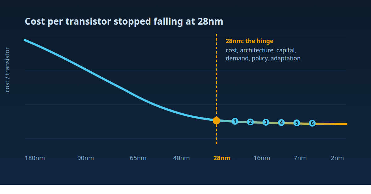
    The 28nm process node is not just old, it is an inflection point in the industry’s history: the node where cost-per-transistor scaling stalled, where planar transistors ended their mainstream run, where fabs split into affordable and unaffordable, where a demand wave arrived, where governments began classifying “mature” chips as a strategic asset, and where engineers kept finding new life in the old design space. Every one of those six shifts changed direction at or near 28nm, which is why a process launched in the early 2010s still carries a large share of the world’s chips.

    We covered the demand side of this story in our earlier piece on why 28nm still rules the world. This post goes deeper on the why: the six inflection points themselves, what each one changed, and how to evaluate 28nm claims the way an analyst would.

    TL;DR

    • Cost: below 28nm, cost per transistor stopped falling reliably (McKinsey, 2013). Design costs roughly doubled from 28nm to 16nm, per IBS estimates.
    • Architecture: 28nm was the last mainstream planar node; Intel’s move to 3-D Tri-Gate transistors at 22nm in 2011 started the FinFET era.
    • Capital: a leading-edge fab now costs tens of billions of dollars; mature-node fabs remain within reach of far more companies (CSET, 2022).
    • Demand: the 2021–2022 chip shortage was concentrated in mature-node parts — MCUs, power-management ICs, sensors — not leading-edge ones.
    • Policy: US export controls now draw the line between “advanced” and “mature” nodes at 16/14nm, and the CHIPS Act set aside $2 billion specifically for legacy chips (CRS).
    • Adaptation: FD-SOI kept the planar transistor alive at 28nm and 22nm with body biasing, proving the node was a design space, not a single recipe.

    What “inflection point” actually means here

    An inflection point is where a trend stops being incremental and changes direction. Moreover, in semiconductor manufacturing they come in three flavors. Physical inflections force an architecture change, like the planar-to-FinFET transition. Economic inflections break the industry’s core bargain, like the stall in cost-per-transistor scaling. Structural inflections reshuffle demand, geography, or policy. The 28nm node sits at the intersection of all three, which explains why it is studied beyond its glamour.

    Inflection 1: cost-per-transistor crossover

    For four decades, the industry’s operating promise was simple: shrink the transistor. Each transistor gets cheaper. That promise underwrote every fab investment. However, McKinsey’s analysis of Moore’s Law found that by the 28nm generation and below, that cost improvement began flattening. Lithography and fab capital costs rose faster than density gains (McKinsey, December 2013).

    The same story shows up in design economics.

    Analyst group IBS estimates a 28nm design cost about $51.3 million.

    A 7nm design costs about $297.8 million, and a 5nm design about $542.2 million (SemiEngineering, 2024).

    Those figures moved.

    An earlier IBS-based estimate for 28nm was $85 million, revised down to about $51 million (SemiEngineering, 2023).

    Thus, below 28nm, design costs rise and per-transistor savings shrink.

    For anything that does not need leading-edge performance, staying at 28nm became the rational financial decision.

    Inflection 2: the planar to FinFET divide

    At 28nm the planar transistor was still the mainstream answer. Intel ended that era in May 2011 when it announced the world’s first 3-D “Tri-Gate” transistors in a production technology, demonstrated on its 22nm Ivy Bridge microprocessor (Intel, May 2011). TSMC, Samsung, and GlobalFoundries followed with 16nm- and 14nm-class FinFET nodes.

    The divide matters because the FinFET transition was expensive twice over: the process got harder, and the design ecosystem had to be rebuilt. IBS-based analysis puts 14/16nm design costs at roughly twice the 28nm figure (SemiEngineering, 2024). IP blocks tuned for planar 28nm could not simply be ported. For analog-heavy and RF-heavy products, that re-authoring cost could erase the entire benefit of the shrink. 28nm became the line the industry stood behind — and, in many product categories, stayed behind on purpose.

    Inflection 3: Who can afford to advance

    The third inflection split the industry into two tiers by capital cost. Similarly, CSET’s January 2022 report estimates leading-edge fabs at roughly $20 billion for a 5nm line. For 3nm, the report lists about $24 billion. For 2nm, the estimate rises to $32 billion, with 35,000 wafers per month (CSET, January 2022). By contrast, the same report estimates legacy-logic fabs costing a fraction of that. It suggests $4–9 billion in incentives could support two to five legacy fabs or upgrades.

    This is the structural heart of the 28nm story.

    A small set of companies can sustain leading-edge R&D and capex.

    Meanwhile, a much larger group operates 28nm-class capacity profitably at far lower capital intensity.

    Depreciation on older fabs is often fully retired.

    So those fabs can profit at wafer prices a leading-edge fab could not survive.

    It also explains apparently contradictory commentary about ‘chip gluts’.

    Mature-node capacity is not fungible with leading-edge capacity, so the two can coexist in shortage and surplus at different times.

    Inflection 4: The demand wave that found 28nm

    The fourth inflection arrived from customers, not from fabs.

    Moreover, the 2021–2022 chip shortage was overwhelmingly a mature-node shortage.

    Industry analysis at the time found microcontrollers, power-management ICs, and image sensors in deepest shortfall.

    Mature-node capacity at major foundries was fully booked and lead times stretched far beyond normal (SemiEngineering, November 2021).

    The reasons are structural. Automotive qualification standards like AEC-Q100 take years to satisfy. Thus, re-qualifying on a new node restarts the clock. Vehicle platforms stay in production for a decade or more. With parts-supply obligations beyond that.

    Many car and factory functions—precision analog, embedded flash, and high-voltage isolation—do not benefit from smaller transistors. Moreover, the shortage made visible what the economics already implied. The chips the world most reliably needed were being built on the nodes nobody writes about. This is evident in the 28 nm Technology Node.

    Inflection 5: geopolitics turns “mature” into a category

    The fifth inflection happened in policy capitals.

    Additionally, since 2022, governments have drawn regulatory lines using node definitions.

    28nm sits on the boundary.

    The US export controls of October 2022 define an ‘advanced-node’ IC as logic at 16/14nm or below with non-planar architectures.

    NAND flash at 128 layers or more, and DRAM at 18nm half-pitch or below are included.

    This explains why mature-node capacity became policy frontier.

    Everything at 28nm and above falls outside that definition.

    The CHIPS Act followed the same logic in subsidy form.

    The Congressional Research Service reports that $2 billion of the initial $19 billion went to legacy chips.

    Additionally, Commerce expects roughly $10 billion to flow to mature and current-generation chips.

    The CRS report also notes it will support specialty technologies and suppliers (CRS R47523).

    China’s buildout of 28nm-and-above capacity mirrors the same classification.

    It is largely with unrestricted tooling.

    When a node’s legal definition drives billions in subsidies and export licenses, mature is no longer a description.

    It has become a category.

    Inflection 6: the FD-SOI fork

    The sixth inflection is the counterargument to the other five.

    28nm was never a single process.

    It was a design space, and engineers kept extracting new value from it.

    FD-SOI keeps the planar transistor.

    It sits on a thin buried oxide.

    Body biasing allows dynamic tuning of the transistor after manufacturing.

    Additionally, GlobalFoundries launched its 22FDX platform in July 2015.

    It promised FinFET-like performance and efficiency.

    This came at a cost comparable to 28nm planar technologies.

    Body biasing was under software control and operation went down to 0.4 volts.

    Moreover, STMicroelectronics built a comparable 28FDX-class offering.

    FD-SOI found real niches in RF, automotive radar, and low-power edge processing.

    The strategic lesson is clear.

    It shows that the node refused to retire and the same lithography generation kept generating new options.

    Moreover, treating 28nm as one fixed product, rather than a family of specialized ones, leads to inaccurate forecasts.

    What the six inflections add up to

    InflectionWhat changed at 28nm
    CostCost-per-transistor scaling stalled; design costs doubled by 16nm
    ArchitectureLast mainstream planar node before FinFET
    CapitalLeading-edge fabs priced out all but a few players
    DemandAutomotive and industrial demand locked onto mature nodes
    Policy28nm became the regulatory boundary for export controls and subsidies
    AdaptationFD-SOI and specialty variants kept the design space alive

    Our view is that the 28nm story is not nostalgia, it is a template. The same argument set — flattening cost curves, qualification lock-in, widening definitions of “legacy” — will re-run at 16nm and eventually 7nm. The companies and analysts who understand it at 28nm first will read the next decade better.

    How to read 28nm claims like an analyst

    Three habits separate useful mature-node analysis from noise. First, check the vintage: much of the cost data still circulating dates from 2013–2015 and has been revised since, sometimes by a third. Second, check what “28nm” means in the specific claim: HKMG logic, BCD power, automotive-qualified MCU, and RF SOI are different products with different pricing. Third, go to primary sources — foundry earnings transcripts, subsidy program documents, and export-control rules — rather than summaries of summaries. Every figure in this post links to one.

    FAQ

    Is 28nm obsolete? No. It remains one of the industry’s highest-volume process families and is frequently the lowest total-cost option once design, mask, and qualification costs are included.

    Why did cost per transistor stop falling below 28nm? Lithography, mask, and fab capital costs rose faster than density gains from 28nm onward, reversing the industry’s four-decade cost trend (McKinsey, 2013).

    What node is the FinFET boundary? Intel introduced 3-D Tri-Gate transistors at 22nm in May 2011; 28nm was the last mainstream planar node.

    How much does a leading-edge fab cost? On the order of $20–32 billion for 5nm through 2nm lines at high volume, versus a fraction of that for mature-node capacity (CSET, 2022).

    Does the CHIPS Act fund mature nodes? Yes. CRS reports $2 billion of the initial $19 billion in manufacturing incentives was set aside for legacy chips, with roughly $10 billion expected to reach mature and current-generation categories.

    Where does 28nm end and “advanced” begin under export controls? The October 2022 US rules define advanced-node logic as 16/14nm or below with non-planar architectures, so 28nm sits well inside the uncontrolled, “mature” category.

  • Thin Films This Week — August 29, 2026

    Thin Films This Week — August 29, 2026

    Three stories this week, and the through-line is film control at scale. Intel is closing the defect-density gap on 14A faster than any node since 22nm, SK hynix is moving the HBM film stack to Indiana, and Kioxia and SanDisk are betting $31 billion that 3D NAND’s dielectric stack is still the roadmap.

    Intel’s 14A Defect Learning Curve Is the Best Since 22nm

    What happened: Intel’s CFO said 14A defect density is dropping faster than the company expected, the best learning-curve performance since 22nm, and that foundry customers have shifted from evaluating data to competing for capacity (Tom’s Hardware, Tech Times, Moomoo).

    Thin films take: For anyone who has spent a decade chasing defect density on leading-edge logic, that CFO line lands hard: 14A is learning faster than anything since 22nm. I know what that means on the floor. It means high-NA EUV single-exposure patterning is holding up, which removes a whole class of overlay and edge-placement defects, but it also means the films underneath are behaving. The high-k gate stack, the work-function metals, and tens of interconnect levels with their barriers, liners, and CMP steps are each a defect generator that has to be tamed in parallel. When customers stop asking for yield data and start asking for capacity, the process control loop has closed faster than the roadmap allowed, and that is a deposition and polish win as much as a litho one. A node’s defect density is a thin-films and CMP story long before it is a litho story.

    SK hynix Breaks Ground on Its First US HBM Base in Indiana

    What happened: SK hynix held the groundbreaking for its first US HBM production base in Indiana, a roughly $4 billion packaging-and-test focused campus targeting mass production around 2028 to 2029, with the CEO calling Indiana a key memory base by 2030 (SK hynix, Reuters, TechPowerUp).

    Thin films take: Groundbreaking in Indiana is where HBM stops being a memory story and becomes a packaging and films story. HBM is built by stacking, and stacking is film engineering: TSVs etched through thinned die and filled with barrier, seed, and copper, hybrid-bonded oxide surfaces polished flat within nanometers, non-conductive films laminated at temperature, and base dies carrying logic-class BEOL. Every stack-height increase multiplies the grind, the deposition, and the bond steps, and each one is a yield event waiting to happen. Standing this up on US soil means duplicating not just the toolset but the recipe book and the people who carry the process knowledge. That is the real multi-year qualification. The yield of an HBM stack is decided at the bond interface, not in the DRAM cell.

    Kioxia and SanDisk Commit $31 Billion to Japan’s 3D NAND Build-Out

    What happened: Kioxia and SanDisk plan to invest more than $31 billion in Japan through 2032 for 3D NAND capacity, led by the new Fab 3 at Kioxia’s Kitakami plant, as AI-driven demand tightens NAND supply and the pair looks to close the gap with Samsung and SK hynix (Bloomberg, The Japan Times, StorageReview).

    Thin films take: More than $31 billion into 3D NAND says the industry still believes the dielectric stack is the roadmap. For films people, 3D NAND is the most deposition-heavy product in the fab: alternating oxide and nitride layers hundreds deep, each interface a potential trap site, each word line a metal fill into an aspect ratio that keeps getting crueler. The move from tungsten to molybdenum word lines, taller ONON stacks, and keeping the stress balanced so the wafer does not bow, that is where the capital actually lands. Kitakami Fab 3 is really a bet that high-aspect-ratio deposition and etch mature faster than the competition’s. 3D NAND is a thin-film deposition business wearing a memory company’s clothes.

  • Thin Films This Week — August 21, 2026

    Thin Films This Week — August 21, 2026

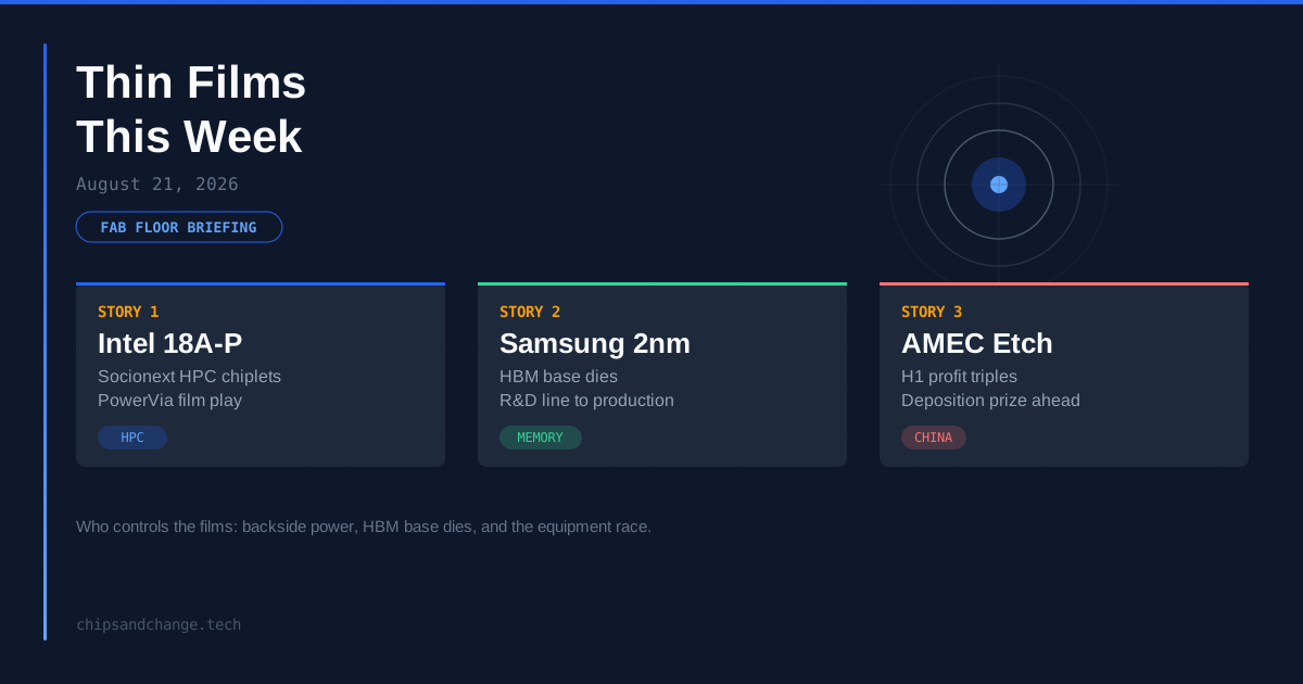
    Three stories this week, and each one is really about who controls the films. Intel signed a serious HPC chiplet customer onto 18A-P, Samsung is pushing HBM base dies to cutting-edge nodes and paying for it with foundry capacity, and China’s AMEC tripled its profit on etch tools while the deposition prize stays out of reach. Same materials physics underneath, three different fabs.

    Intel Lands Socionext for 18A-P High-Performance Compute Chiplets

    What happened: Japanese custom-SoC house Socionext will build high-performance compute chiplets on Intel’s 18A-P process, adding Intel Foundry as a second source alongside TSMC, and its shares slid more than 5 percent as investors weighed the economics of the deal (New Electronics, TrendForce, digitimes).

    Thin films take: For those of us who have spent years qualifying backside power, 18A-P is the process I point to when people ask what actually changed at Intel. The ribbonFET channels are demanding enough: conformal ALD of the high-k stack and TiN work-function metal across four or five stacked nanosheets, with precursor depletion fighting you at the bottom of the stack. But PowerVia is the film play. You grind the wafer, etch through the substrate, and build a second interconnect network on the backside, which means thick stress-balancing dielectrics, deep via fills, and a wafer that wants to bow every way at once. The yield limiter on backside power was never litho, it was film stress and wafer flatness. A designer like Socionext signing off on 18A-P for chiplets says Intel’s backside stack is finally stable enough to bet a product on. 18A-P’s credibility rests on a backside film stack that stays flat enough to keep every subsequent litho level in focus.

    Samsung Repurposes an R&D Line for 2nm HBM Base Dies

    What happened: Samsung is reportedly converting a foundry R&D line into production capacity targeting cutting-edge 2nm HBM base dies in anticipation of future NVIDIA demand, extending its 4nm HBM4 base-die roadmap, and will break ground on a KRW 6 trillion Onyang HBM fab in September (TrendForce, Wccftech, TrendForce).

    Thin films take: The HBM base die is quietly becoming the most interesting film stack in memory, because it is logic-class BEOL bolted onto a DRAM supply chain. Moving it to 2nm means finer pitches, lower-k dielectrics, and a lot more ALD content, all on a wafer that will later be ground to tens of microns, punched with TSVs, and bonded. Everything downstream lives or dies on stress engineering: the BEOL films have to survive backside grind without cracking, the TSV barrier and seed have to go down void-free, and the top Cu-in-dielectric bond surface has to be flat within nanometers so the oxide-to-oxide bond wets out. Repurposing an R&D line tells me Samsung is compressing the qual cycle, proving the 2nm base-die process before Onyang breaks ground. Film stress and wafer warpage, not transistor performance, are what gate the 2nm HBM base die.

    AMEC Triples H1 Profit as China’s Etch Beachhead Grows

    What happened: China’s AMEC reported first-half net profit tripling to 2.83 billion yuan with plasma-etch profit nearly doubling, and announced a 3.5 billion yuan Phase II expansion of its Lingang industrialization base, as its tools gain share in Chinese fabs while TSMC phases them out (Moomoo, finance.biggo, Tech Times).

    Thin films take: I have watched AMEC go from the MOCVD supplier nobody wanted to the etch vendor Chinese fabs actually depend on, and this week’s numbers say the transition is working. Tripling first-half profit on plasma etch, with SMIC having bought 800-plus machines, is the beachhead. But here is what gets my attention as a films person: etch was always the easier entry point, the real prize in equipment localization is deposition, and AMEC’s roadmap has been creeping from etch into CVD, ALD, and epitaxy for years. The 3.5 billion yuan Lingang Phase II spend is them scaling the industrialization base to chase exactly that. TSMC phasing AMEC tools out of its fabs is the market telling them they are not yet a front-end films house, and that gap is measured in film uniformity, defect density, and process control data that takes years to accumulate. China’s equipment localization story is an etch story today, but the deposition prize is what the Lingang expansion is really buying.

  • Thin Films This Week — August 14, 2026

    Thin Films This Week — August 14, 2026

    This week the money moved through the machines. Applied Materials printed a record quarter on AI deposition demand, TSMC pushed CoWoS-L to 98 percent yield at 5.5x reticle, and Samsung crossed the golden-yield line on HBM4. Three business headlines, and each one is a thin films story underneath.

    Applied Materials: Record Quarter, Six New AI Systems, and a Margin Grumble

    What happened: Applied Materials posted record Q3 revenue of $9.12B with earnings above estimates and guided Q4 to $10.25B, yet shares fell about 5 percent as investors wanted faster growth from the AI equipment winner; the company also introduced six new systems for AI chipmaking (Reuters; 24/7 Wall St.).

    Thin films take: I have watched Applied Materials’ order book long enough to remember when a billion-dollar deposition quarter was an event. Now it is a baseline. Record $9.12B, a $10.25B guide, six new systems for AI chipmaking: Endura-class PVD and Producer-class CVD being pulled through the door by GAA and backside power delivery. The margin grumble, 50.4 percent gross and flat, misses the point. Mix shifts as AI logic pulls in more ALD and high-aspect-ratio CVD, and the new systems target the film stacks that decide N2 yields: conformal metal gates, low-k spacers, the thick dielectric build on the backside. When the deposition house prints record quarters two years into a node transition, film count per wafer is still climbing. The AI buildout has become a materials-engineering capex story, and deposition is the biggest line item in it.

    TSMC Hits 98% Yield on CoWoS-L at 5.5x Reticle, 14x Comes in 2029

    What happened: TSMC has reached 98 percent yield on CoWoS-L interposers at 5.5x reticle size, with a 14x reticle generation on the roadmap for 2029 (TechPowerUp).

    Thin films take: CoWoS-L at 5.5x reticle is not a packaging headline, it is a thin films achievement. A reticle-scale interposer means one RDL field with Cu lines and SiO2 or polymer dielectric that has to stay uniform across an area that used to be five separate die. At that scale the yield killers are film thickness spread, Cu plating nodulation, and dielectric pinholes, not litho. 98 percent says the dielectric deposition and CMP are holding flatness and defectivity across the whole field, and that the stitching boundaries are invisible to plating. The 14x jump in 2029 will stress every deposition and planarization step again, and hybrid bonding on top means the top dielectric surface becomes the device. 98 percent at 5.5x reticle is a dielectric uniformity and CMP story, and 14x in 2029 is the next stress test.

    Samsung Reports 80% “Golden Yield” on HBM4, Accelerates HBM4E

    What happened: Samsung has reportedly hit an 80 percent “golden yield” on HBM4 production as it pushes to take AI DRAM share from SK Hynix, and is speeding up HBM4E development (Wccftech; Seoul Economic Daily).

    Thin films take: Golden yield on HBM4 is a stack-level statement, but the work is all films and interfaces. A 16-high stack carries thousands of TSVs, and each one needs a TaN/Ta barrier and Cu seed that PVD lays down void-free, plus a dielectric fill that does not crack. The step that usually owns HBM yield is the bond interface: MR-MUF with NCF for the bulk, with hybrid bonding creeping in from the base die as HBM4E ramps. 80 percent means deposition and planarization are playing at DRAM-grade defect densities across 16 die, and that film-stack warpage is under control through reflow. Samsung speeding up HBM4E says they trust the film work enough to compress the product cycle. 80 percent on 16-high means the TSV fill and the bond interface are both qualified at volume, and the rest is a market share question.

  • Thin Films This Week — August 7, 2026

    Thin Films This Week — August 7, 2026

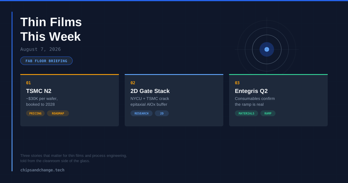
    Another week where the leading edge got more expensive and the research floor got more interesting. Three stories with real process implications: TSMC’s N2 pricing crossing $30,000 a wafer, a gate-stack breakthrough for 2D channels out of NYCU and TSMC Corporate Research, and an earnings print from the consumables layer that confirms the ramp is real.

    TSMC’s N2 Wafer Hits ~$30,000, and the Order Book Runs to 2028

    What happened: TSMC’s 300mm N2 wafers are now priced around $30,000 each, up from $18,000 to $20,000 at N3, with N2 and A16 capacity booked out to 2028 while 3nm wafer starts climb toward 180,000 a month by early Q4, two to three months ahead of schedule (tech-insider.org; TrendForce).

    Thin films take: The headline read is supply and demand, and that is true. But the node-to-node jump is mostly a film-stack story. A GAA wafer carries more deposited layers than any FinFET: conformal ALD wrapping four nanosheet channels, inner spacers, a TiN work-function metal now tuned per device instead of per node, low-k spacer films, and the superlattice epi the channels are etched out of. Film count per wafer has roughly doubled since N5. TrendForce’s pushback, that the real increase is closer to 10 to 20 percent once customer tiers are counted, matches what I see on the floor: the added cost is deposition and etch time, not litho. And A16 at a rumored $45,000 adds backside power delivery, which means carrier bonding, a backside grind, and an entire backside film stack with re-passivation. Wafer bow from those thick backside films will be the next yield fight, and the teams that control stress in the dielectric stack will earn their keep.

    NYCU and TSMC Crack the 2D Gate Stack with an Epitaxial AlOx Buffer

    What happened: Researchers at National Yang Ming Chiao Tung University and TSMC Corporate Research demonstrated monolayer MoS2 top-gate transistors combining a gate dielectric with about 1nm equivalent oxide thickness and 0.45 mS/um maximum transconductance, using an epitaxial aluminum layer on CVD-grown MoS2 oxidized into a 0.42nm AlOx buffer under HfO2 (SciTechDaily; Nature Electronics).

    Thin films take: This is the nucleation problem I have fought for a decade. A 2D channel has no dangling bonds, so ALD on MoS2 nucleates in islands: pinholes, interfacial charge, mobility collapse. We have tried ozone pulses, plasma pretreats, and polymer seeds, and the EOT, control, and transport triangle never closes. The NYCU move is elegant because a metal wets the van der Waals surface epitaxially, and oxidation gives a self-limiting, atomically smooth AlOx that HfO2 can actually grow on. 0.42nm of buffer under high-k, about 1nm EOT, low hysteresis, 0.45 mS/um on a 100nm channel: that combination has been the blocker for 2D logic. And the channel is CVD-grown monolayer, not an exfoliated flake, so there is a wafer-scale path. An oxidized epitaxial metal may be the seed layer that makes 2D gate stacks manufacturable, the kind of interface work that decides whether MoS2 ever reaches a high-volume line.

    Entegris Q2: The Consumables Layer Confirms the Ramp Is Real

    What happened: Entegris beat across the board with $883.2M in Q2 revenue, up 11% year over year, and adjusted EPS of $0.93, up 41%, as AI demand reached the materials layer: Advanced Purity Solutions grew 17% to $514.6M with margin expanding 620 basis points to 30.3%, and Q3 was guided to $905M to $935M (Tech Times).

    Thin films take: Materials suppliers are the canary in the fab. Entegris is roughly 95% consumables: deposition precursors, filtration membranes, CMP slurries, specialty gases. When that book grows 11% and EPS grows 41%, the mechanism is fab utilization showing up in the BOM, not hype. The compounding driver is content per wafer. GAA at N2 means more ALD steps, so more precursor drums, more filter change-outs, more slurry per wafer. HBM stacks add TSV barrier deposition and dielectric fill, and every one of those steps runs a qualified material with years-long switching costs baked in. I have lived those qualifications; once a membrane is in the flow, you do not swap vendors mid-ramp. Per-wafer materials consumption, not wafer count, is the growth curve to watch this cycle, and it is still climbing.

  • Thin Films This Week — July 31, 2026

    Thin Films This Week — July 31, 2026

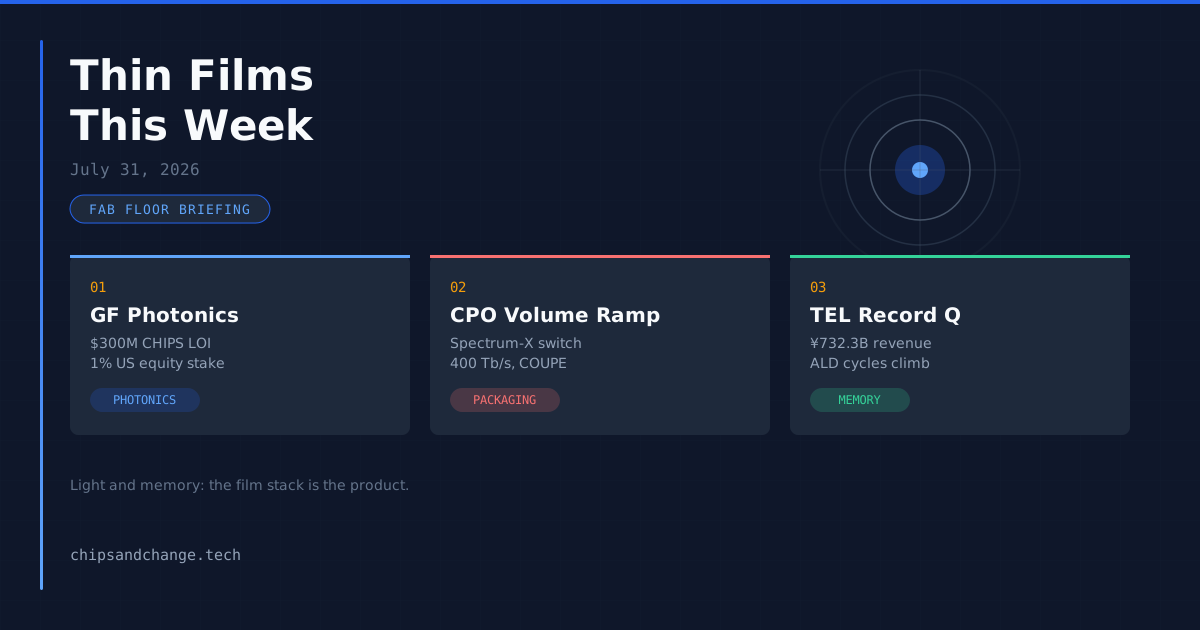
    Welcome to this week’s Fab Floor Briefing: three stories that matter for thin films and process engineering, told from the cleanroom side of the glass. This week is all about light and memory, two businesses where the film stack is the product.

    1. Washington Buys Into GlobalFoundries’ Photonics Bet: $300M CHIPS LOI, 1% Stake, CPO Front and Center

    What happened: GlobalFoundries signed a letter of intent with the US Department of Commerce for a $300 million CHIPS R&D award to accelerate its silicon photonics program, with the government taking a 1% equity stake and the work emphasizing co-packaged optics for AI data centers.

    Thin films take: Silicon photonics is a thin films business wearing a chip company’s clothes. The passive backbone is a PECVD silicon nitride core in a silica cladding, and the receiver side is selective germanium epitaxy in oxide windows for the photodetectors. I’ve run 300 mm SiPh flows, and the pain is never the waveguide itself, it’s the thermal budget: you deposit and anneal these films after the FEOL dopants are already in, so the reflow tricks from interlevel dielectric work are off the table. The government taking equity tells me Washington now treats photonics capability the way it treats fabs, as a national-security asset. For process engineers that means funded lines for SiN deposition, Ge epi, and edge-coupler CMP on GF’s 45 nm SOI platform. Waveguide loss is the yield metric that matters: every 0.1 dB/cm shaved in the PECVD nitride is capacity you never have to build.

    Source: SiliconANGLE · Semiconductor Digest

    2. CPO Crosses Into Volume Ramp, and the Optical Engine Becomes a Yield Problem

    What happened: TrendForce reports NVIDIA has begun shipping its Spectrum-X CPO switch, co-developed with TSMC using COUPE packaging and rated up to 400 Tb/s, while Broadcom volume-ramps its 51.2T Bailly switch, with optical engine yield, silicon photonics fab capacity, and advanced packaging availability flagged as the three bottlenecks to expansion.

    Thin films take: Every CPO roadmap hits the same wall: the optical engine is a thin films stack with a laser bolted on. You’re hybrid-bonding a photonics die to the switch ASIC, and the bond interface is Cu pads on SiO₂, which means the whole package lives or dies on CMP. One micro-scratch, one dishing hotspot on the bonding surface, and that die is scrap before it ever sees light. I’ve watched die-to-wafer hybrid bonding teams chase particle specs that would make a logic fab blush: a single 0.5 µm defect on the bond surface can kill the optical path, and there is no rework. Add laser arrays dumping heat next to the switch, and the underfill and lid materials start dictating the package design. Hybrid bonding surface prep is where CPO yield goes to die: one micro-scratch in the oxide and that optical engine is a light fixture, not a transceiver.

    Source: TrendForce

    3. TEL’s Record Quarter Says the Memory Film Stack Isn’t Done Growing

    What happened: Tokyo Electron posted record revenue of ¥732.3 billion in FY2027 Q1 (April through June 2026) and raised its first-half net profit forecast to ¥349 billion on July 30, citing AI data center investment and strong memory chip demand.

    Thin films take: For anyone who thinks memory capex has peaked, TEL’s numbers are the tell. A record quarter built on DRAM and HBM demand means one thing from where I sit: more ALD cycles. Every DRAM generation pushes the capacitor higher in aspect ratio and the high-k stack thinner, and the word line keeps eating tungsten. Those are deposition-intensive structures, and TEL’s Triase ALD and CVD line is the default answer for a big share of them. HBM adds its own film tax: TSV liners, tungsten fill, backside redistribution. I’ve lived through three memory supercycles, and the tool that sells first in an AI-driven upcycle is always the deposition tool, because every bit of new memory capacity is a film stack first, and TEL’s beat-and-raise says the deposition content per wafer is still climbing.

    Source: DigiTimes · Investing.com

    That’s the floor for this week. Keep your precursors cold and your ellipsometer calibrated.

  • Thin Films This Week — July 27, 2026

    Thin Films This Week — July 27, 2026

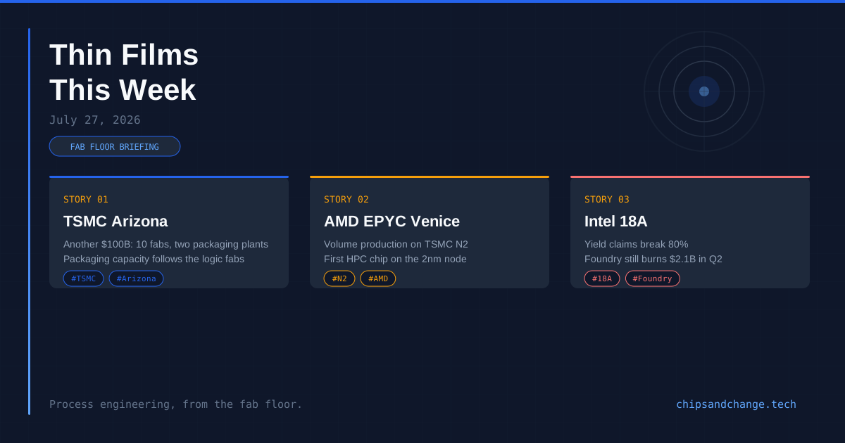
    Welcome to this week’s Fab Floor Briefing — three stories that matter for thin films and process engineering, told from the cleanroom side of the glass.

    1. TSMC Drops $100B More on Arizona — 10 Fabs, Two Packaging Plants, and a Whole Lot of Dep Kit

    What happened: TSMC announced an additional $100 billion investment in its Arizona campus on July 22, bringing total commitment to $265 billion across 10 wafer fabs, two advanced packaging facilities, and an R&D center — the largest single-site semiconductor investment in history.

    The thin films take: Ten fabs means ten times the CVD, PVD, and ALD chamber installs I’ll be qualifying over the next decade. The scale here isn’t just about more wafers — it’s about what kinds of films they’ll be running. TSMC’s Arizona roadmap has to mirror Taiwan’s node progression, which means N2 high-NA EUV patterns with sub-1nm ALD high-k gate dielectrics, cobalt liners replacing tungsten at contact levels, and hybrid bonding dielectric stacks for the advanced packaging lines. I’ve been through a greenfield fab startup before, and the nightmare isn’t the tool install schedule — it’s the process-of-record transfer from Taiwan. Every angstrom-level film thickness recipe that works in Hsinchu’s humidity profile needs re-qualification in Phoenix desert conditions. The ALD HfO₂ cycles that yield 15.2 Å at 50% RH in Taiwan might give you 16.1 Å here. That’s weeks of TEM cross-sections and inline ellipsometry to nail back down.

    Source: Engineering News-Record · Fast Company

    2. AMD’s EPYC Venice Hits Volume Production on TSMC 2nm — First HPC Chip on N2

    What happened: AMD announced at Advancing AI 2026 on July 23 that its 256-core EPYC Venice processor has entered volume production on TSMC’s 2nm (N2) node — the industry’s first high-performance computing chip to reach this milestone on the advanced process.

    The thin films take: N2 is TSMC’s first node to go all-in on gate-all-around (GAA) nanosheets with a full nanosheet gate stack that demands conformal ALD deposition across 4-5 stacked channels — not the planar FinFET architecture we’ve been married to for a decade. From a thin films perspective, this is where the real action is: the inner spacer nitride deposition, the high-k/metal gate stack conformality requirement across those suspended silicon channels, and the work-function metal tuning that now has to happen on four discreet nanosheet surfaces instead of a single fin. The margin for error in equivalent oxide thickness (EOT) just got cut in half. I’ve been watching the N2 ALD precursor pipeline for the past 18 months, and the shift to new metal-organic precursors for the gate stack is the kind of change that keeps process integration up at night. If the TiN work-function layer on the bottommost nanosheet is 17 Å but only 14 Å on the top sheet because of precursor depletion in a high-aspect-ratio structure, you’ve got Vt mismatch across channels. The ALD saturation curves that worked on planar and FinFET don’t transfer to nanosheets — period.

    Source: AI Weekly · TechPowerUp

    3. Intel Foundry Claims 18A Yield Breaks 80% — But Still Burns $2.1B in Q2

    What happened: Intel reported Q2 2026 earnings on July 23 showing Foundry revenue of $5.76 billion (up 31% YoY) with an operating loss narrowing to $2.1 billion, while 18A yield reportedly surged to 85% — up from 65% the prior quarter — and internal volume targets were exceeded.

    The thin films take: 18A is Intel’s first node built around RibbonFET (their GAA implementation) and PowerVia backside power delivery. From where I sit, the yield jump from 65% to 85% tells me the deposition community figured out the backside contact film integration challenge. PowerVia buries the power rails under the wafer, which means you’re now depositing and annealing films on both sides of the wafer — a thermal budget nightmare if I’ve ever seen one. The dielectric films on the frontside nanosheet stack and the backside isolation layers now share a single thermal cycle, and any film stress mismatch between the frontside SiN liner and the backside SiO₂ isolation will warp the wafer badly enough that the scanner can’t hold focus on the overlay targets. I’d bet the yield unlock came from tuning the PECVD TEOS oxide stress on the backside to cancel the compressive stress from the frontside high-k/metal gate stack. That kind of film stress engineering — balancing frontside and backside deposited films across a 775µm substrate — hasn’t been done at production scale before. The $2.1B loss still stings, but the yield trajectory is credible.

    Source: FourWeekMBA · VendorDeep · Yahoo Finance


    That’s the floor for this week. Keep your precursors cold and your ellipsometer calibrated.

  • Thin Films This Week — July 17, 2026

    Thin Films This Week — July 17, 2026

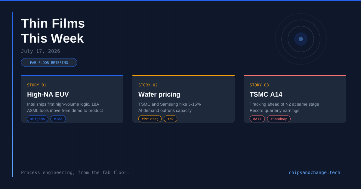
    Three stories from the fab floor this week that matter for thin films and process engineering.

    1. Intel Ships First High-Volume Logic Chips Using ASML High NA EUV on 18A

    What happened: Intel became the first company to ship high-volume logic products using ASML’s High NA (0.55 NA) EUV lithography, with select Panther Lake layers on Intel 18A now dual-qualified across both NXE and EXE scanner platforms. Thin films take: This is the one I’ve been waiting for — not because of the optics, but because of what High NA does to the resist stack. At 0.55 NA, you’re pushing 8 nm half-pitch resolution, which means the photoresist thickness budget collapses. We’re now running sub-30 nm resist films on production wafers, and the etch selectivity problem becomes your new best friend and worst enemy. The dual-qualification is the sleeper here: same layer runs on either 0.33 NA or 0.55 NA, which means the hardmask stack — the SiON, the spin-on carbon, the anti-reflective layers — all had to be re-engineered to be scanner-agnostic. I’ve spent enough nights in the fab fighting reflectivity swings from a single-nm change in anti-reflective coating thickness to know how much work that took. The resist and underlayer film vendors just earned their keep this quarter.

    2. TSMC and Samsung Hike Advanced Node Wafer Prices 5-15% as AI Demand Outpaces Capacity

    What happened: TSMC raised wafer prices 5-10% across 3nm, 5nm, and 7nm nodes while Samsung selectively hiked 4nm, 5nm, and select 8nm automotive nodes by up to 15%, marking a structural shift from a buyer’s to a seller’s foundry market. Thin films take: Every time I see a wafer price hike headline, I think about the consumables budget. The deposition materials cost per wafer at 3nm has tripled versus 7nm — the ALD cycle count alone for the gate stack, the work-function metal layers, the multiple threshold-voltage Vt tuning films — it adds up fast. At 3nm, a single wafer goes through 80+ ALD cycles before you ever get to the first metallization step, and each cycle burns precursor that costs more per gram than silver. The price hikes aren’t just about EUV tool depreciation; they’re a direct reflection of film stack complexity. I’ve seen PVD targets for advanced nodes now cost 4x what they did at 28nm because the purity spec went from 5N to 6N5 and the grain size uniformity requirement tightened. Samsung’s selective pricing — only on 4nm and 5nm — tells me they’re still struggling with GAA film uniformity at SF2 yields, and they can’t justify a blanket hike until they solve the nanosheet epitaxial layer thickness control. That’s a deposition problem, plain and simple.

    3. TSMC A14 (1.4nm) Progress Well Ahead of N2 at Same Stage, Record Quarterly Earnings

    What happened: TSMC confirmed on its Q2 2026 earnings call that its A14 (1.4nm-class) process development has surpassed N2’s trajectory at the equivalent stage, with significant yield and performance improvements, and reported a record quarterly profit driven by insatiable AI chip demand. Thin films take: A14 going faster than N2 at the same stage is the kind of comment that either means you’ve solved your (1,0,0) vs (1,1,0) nanosheet orientation problem, or you haven’t and you’re talking around it. I’ll bet it’s the former. The film stack at 1.4nm requires gate-all-around with channel thickness control to within ±0.3 nm across a 300 mm wafer — that’s roughly two atomic layers of silicon — and the fact that TSMC is publicly claiming “significant yield improvements” on A14 means their SiGe epitaxial release layer etching and the subsequent channel release are landing within that window. For those of us in process integration, the really interesting part is how they’re managing the MOL (middle-of-line) contacts at this pitch. At 1.4nm, the contact CD is pushing below 12 nm, and you cannot get conformal TiN liner coverage with PVD anymore — you’re all-in on ALD TiN, and the resistivity penalty from the higher carbon content in the ALD-deposited film versus PVD is a constant tradeoff I don’t envy their integration team. Record earnings help pay for the 10,000 wafer experiments it’s going to take to dial that in.
  • Thin Films This Week — Friday, June 5, 2026

    Thin Films This Week — Friday, June 5, 2026

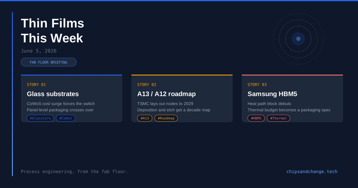
    1. Glass Substrates Cross the Inflection Point — CoWoS Cost Surge Accelerates the Tectonic Shift

    What happened: TrendForce published a landmark assessment on June 5 confirming that glass core substrates are targeting 2027 commercial launch and scaling toward mainstream adoption by 2030. The catalyst: CoWoS packaging costs have surged to $750–1,100 per chip, and hyperscaler demand for next-generation infrastructure is now the primary driver. Intel, SKC/Absolics, Samsung Electro-Mechanics, and the recently announced Intel-Odisha $3.3B India facility are all racing toward volume production.

    Thin films take: This is the week the industry stopped asking “if” and started asking “when” for glass substrates, and if you’ve spent your career in PVD and wet-etch processes, you should be paying close attention — because everything changes when your substrate goes from organic laminate to borosilicate glass. The TrendForce report puts it plainly: silicon interposer yield losses on packages above 2,700mm² are driving CoWoS-L costs 20–40% higher than CoS, and glass substrates eliminate the interposer entirely. But from where I sit, the real thin-films story is the TGV (through-glass via) process. Standard reactive ion etch recipes that work beautifully on silicon dielectrics don’t transfer to glass — the etch chemistry, the sidewall angle control, the barrier seed layer adhesion — every deposition sequence in the packaging flow has to be revalidated for a glass substrate, and the dielectric build-up on glass defines defect density for the whole module. The Intel Odisha facility combined with the TrendForce timeline means we’ll see pilot-scale TGV PVD tool evaluations inside 18 months. If you’re a process integration engineer who hasn’t run a DOE on Ti/Cu seed adhesion to alkaline earth boroaluminosilicate glass yet, your calendar just got full.

    Sources: TrendForce — Glass Substrates Eye 2027 Launch (Jun 5, 2026); SiliconAnalysts — CoWoS Packaging Cost: $750–1,100/Chip (Apr 2026); Intel Rio Rancho — Glass Substrate Mass Production Targets

    2. TSMC Debuts A13/A12 Roadmap to 2029 — Deposition and Etch Engineers Get Their Next Decade of Work

    What happened: At the 2026 North America Technology Symposium in Santa Clara (April 22–23), TSMC unveiled a roadmap extending through 2029 with A13 (1.3nm-class) and A12 (1.2nm-class) nodes. A13 promises 6% area reduction over A14, while A12 pushes further with continuous nanosheet architecture refinement and backside power delivery evolution. The roadmap also includes N2U (N2 with buried power rail), expanded CoWoS interposer sizes up to 9.5X reticle, and the SoW-X wafer-scale integration platform for next-gen AI training. A16 enters volume production in H2 2026 in Taiwan, with Arizona A16 production targeted for 2028.

    Thin films take: Every TSMC roadmap refresh since A16 has leaned harder on backside power delivery, and A13/A12 are no exception. The Super Power Rail architecture — moving the power distribution network to the wafer backside — means we now need to deposit dielectric liners and Cu fill into via-middle structures that are etched from the back of a thinned wafer, with aspect ratios that push conventional PVD and CVD beyond their existing chamber hardware capabilities. A16 already requires >500 process steps per GAA transistor, and A13/A12 will add more — each angstrom-level shrink introduces additional spacer layers, workfunction metal tuning steps, and dielectric stack complexity that show up in every CVD and ALD chamber’s preventive maintenance schedule. The symposium also confirmed that TSMC does not believe high-NA EUV is required for A14, meaning the industry’s multi-patterning workload stays high — which is good news for anyone whose job security depends on running ASML NXE:3800E scanners at full utilization. And on the packaging side, the expanded CoWoS interposer roadmap (9.5X reticle by 2027) means the PVD seed layers and electroless Cu processes for those massive interposers become yield-limiting steps that demand chamber uniformity specs that today’s tools can barely hit across a 300mm wafer, let alone a reticle-scale interposer.

    Sources: Cloud News — TSMC extends its lead until 2029 with A13, A12; New Electronics — TSMC Technology Symposium 2026; Insider Monkey; Tech-oracle.com

    3. Samsung HBM5 Introduces Heat Path Block — A Packaging Thermal Challenge That Becomes a Thin-Films Problem

    What happened: At COMPUTEX 2026 (June 2), Samsung unveiled the world’s first HBM5 mock-up, featuring a proprietary thermal management technology called Heat Path Block (HPB). HBM5 uses a 2nm base die (manufactured in-house at Samsung Foundry) and supports 12, 16, and 20-layer DRAM stacks. HPB adds dedicated thermal pillars that pull heat from inside the stacked dies — essentially a through-silicon via (TSV) architecture repurposed for thermal conduction rather than electrical interconnect. Volume production is projected around 2028, with Nvidia still uncommitted (SK Hynix remains the preferred HBM supplier).

    Thin films take: Samsung’s HPB is a structure that exists entirely because the thin-films interfaces in HBM stacks can’t move heat fast enough. Here’s the physics: as HBM stacks go from 8 to 12 to 20 layers, the cumulative thermal resistance of the dielectric bonding layers — the SiO₂ or SiCN hybrid bond interfaces between each DRAM die — becomes the dominant heat transfer bottleneck. Every 10nm of dielectric between Cu hybrid bond pads adds measurable thermal impedance, and at 20 layers you’re looking at a total dielectric stack that can exceed 1µm of oxide between the hottest die and the package lid. HPB adds dedicated Cu thermal TSVs that bypass those dielectric interfaces entirely — but that means Samsung now needs to integrate thermal TSVs into the DRAM memory cell array processing flow, which they’ve never had to do before in HBM. The TSV etch for thermal vias is different from signal TSVs: lower aspect ratio but larger critical dimension, which changes the scalloping profile requirements on the Bosch etch process. And the dielectric liner deposition for thermal TSVs must balance electrical isolation (you don’t want Cu diffusion into DRAM cells) against thermal conductivity (too much liner and you’ve just recreated the problem you’re solving). For the process engineers at Samsung’s HBM line in Pyeongtaek, HPB means a whole new thin-films integration flow in the TSV module — and given that Samsung is already struggling to match SK Hynix’s HBM yields, adding a new thermal TSV process to the flow is a high-risk, high-reward bet.

    Sources: Tom’s Hardware — Samsung shows first HBM5 mockup with HPB (Jun 2, 2026); TechTimes — HBM5 Debuts at Computex; Korea Times; Chosun Biz (Jun 2, 2026)

  • Thin Films This Week — Friday, May 29, 2026

    Thin Films This Week — Friday, May 29, 2026

    Friday, Friday, May 29, 2026

    Three stories caught my eye this week — each one a reminder that what looks like business news from the outside is, on the fab floor, a thin-films problem waiting to be solved.

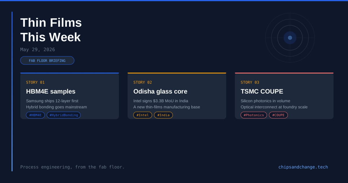
    1. Samsung Ships World’s First HBM4E 12-Layer Samples — Hybrid Bonding Goes Mainstream

    What happened: Samsung Electronics began shipping the industry’s first 12-layer HBM4E samples to global customers on May 29, delivering 16 Gbps per pin (20% faster than HBM4), 48 GB capacity per stack, and 3.6 TB/s bandwidth — pulling ahead of SK Hynix and Micron on the next-generation HBM roadmap.

    Thin films take: For those of us who’ve spent years fighting Cu pillar coplanarity on thermal compression bonders, HBM4E at 12 layers means the hybrid bonding transition is no longer theoretical — it’s in customer hands. Moving from microbump to Cu-Cu hybrid bonding at this stack height changes everything about the dielectric deposition flow. You’re no longer trying to keep 25µm solder bumps uniform across a 12-high stack; you’re now controlling a 500nm dielectric CMP process across a bonded interface that has to survive thermal cycling at under 1µm total stack bow. Samsung is running this on 1α-class DRAM, which means the buried bitline and capacitor contacts underneath have their own thermal budget constraints. The dielectric gap-fill for the hybrid bond interface at 12 layers is now the yield-limiting process step — not the DRAM cell itself. I’ve been watching HBM process integration since HBM2, and this is the first generation where the bonding layers dictate more of the final yield than the memory arrays.

    2. Intel Signs $3.3B Glass Core Substrate MoU with Odisha, India — A New Thin-Films Manufacturing Frontier

    What happened: Intel and 3D Glass Solutions (3DGS) signed a $3.3B MoU with the Government of Odisha on May 29 to build an advanced packaging glass core substrate manufacturing facility near Bhubaneswar — one of India’s largest high-tech manufacturing investments — targeting 1,800+ jobs in a first-of-its-kind Indian project for substrate-level packaging.

    Thin films take: Glass core substrates are where the thin-films community gets to reinvent everything we thought we knew about packaging. If you’ve ever dealt with organic substrate warpage on a 100mm×100mm package body, you know why foundries are desperate for a replacement: BT resin and Ajinomoto build-up films just can’t hold flat at the reticle sizes AI accelerators demand. Glass changes the game, but it brings a whole different set of deposition challenges. Getting metal adhesion layers to stick to bare glass at the 2/2µm L/S that advanced packages now require means we have to completely rethink the PVD seed and electroless Cu sequences that have been standard on organic substrates for two decades. 3DGS brings their TGV (through-glass via) expertise, which is a wet-etch + dry-film laminography process that most of the semi world hasn’t touched. I’ll be watching how they handle the dielectric build-up on glass — that interface between the glass carrier and the first redistribution layer is going to define defect density for the whole module.

    3. TSMC COUPE Silicon Photonics Begins Volume Production — Foundry-Scale Optical Interconnects Arrive

    What happened: TSMC’s COUPE (Compact Universal Photonic Engine) platform is entering volume production in H2 2026, with AMD as the initial adopter, and Nvidia’s Rubin Ultra likely to follow — while Samsung’s rival silicon photonics foundry platform targets 2028 mass production and 2029 CPO turnkey, according to Commercial Times and Ming-Chi Kuo analyses.

    Thin films take: Silicon photonics at foundry scale is a thin-films integration problem dressed up as an optics play. COUPE’s first-generation die — the one AMD is taping out now — stacks a photonic IC (PIC) directly on top of an electrical IC (EIC) using TSMC’s own hybrid bonding. That means your standard 300mm fab line is now running SiN waveguide deposition, Ge epitaxy for photodetectors, and oxide cladding layers through tools that used to be reserved for Cu damascene and ILD. The SiN film stress uniformity across a 300mm wafer for a waveguide core that has to maintain ±1nm thickness variation over centimeters of spiral path is tighter than anything most PECVD chamber apps have been asked to deliver. And the edge coupler — where light enters from a fiber — requires a facet etch through multiple dielectric stacks with a sidewall angle tolerance that makes gate spacer etch look like rough carpentry. This is where the thin-films world collides with photonics-grade process control, and the overlap in capability sets is still thin on the ground. If you’re a deposition engineer who hasn’t started thinking about SiN film stress engineering for photonic waveguides, your next performance review may be an uncomfortable one.

    — Your Fab Floor Correspondent