
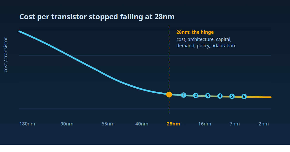
The 28nm process node is not just old, it is an inflection point in the industry’s history: the node where cost-per-transistor scaling stalled, where planar transistors ended their mainstream run, where fabs split into affordable and unaffordable, where a demand wave arrived, where governments began classifying “mature” chips as a strategic asset, and where engineers kept finding new life in the old design space. Every one of those six shifts changed direction at or near 28nm, which is why a process launched in the early 2010s still carries a large share of the world’s chips.
We covered the demand side of this story in our earlier piece on why 28nm still rules the world. This post goes deeper on the why: the six inflection points themselves, what each one changed, and how to evaluate 28nm claims the way an analyst would.
TL;DR
- Cost: below 28nm, cost per transistor stopped falling reliably (McKinsey, 2013). Design costs roughly doubled from 28nm to 16nm, per IBS estimates.
- Architecture: 28nm was the last mainstream planar node; Intel’s move to 3-D Tri-Gate transistors at 22nm in 2011 started the FinFET era.
- Capital: a leading-edge fab now costs tens of billions of dollars; mature-node fabs remain within reach of far more companies (CSET, 2022).
- Demand: the 2021–2022 chip shortage was concentrated in mature-node parts — MCUs, power-management ICs, sensors — not leading-edge ones.
- Policy: US export controls now draw the line between “advanced” and “mature” nodes at 16/14nm, and the CHIPS Act set aside $2 billion specifically for legacy chips (CRS).
- Adaptation: FD-SOI kept the planar transistor alive at 28nm and 22nm with body biasing, proving the node was a design space, not a single recipe.
What “inflection point” actually means here
An inflection point is where a trend stops being incremental and changes direction. Moreover, in semiconductor manufacturing they come in three flavors. Physical inflections force an architecture change, like the planar-to-FinFET transition. Economic inflections break the industry’s core bargain, like the stall in cost-per-transistor scaling. Structural inflections reshuffle demand, geography, or policy. The 28nm node sits at the intersection of all three, which explains why it is studied beyond its glamour.
Inflection 1: cost-per-transistor crossover
For four decades, the industry’s operating promise was simple: shrink the transistor. Each transistor gets cheaper. That promise underwrote every fab investment. However, McKinsey’s analysis of Moore’s Law found that by the 28nm generation and below, that cost improvement began flattening. Lithography and fab capital costs rose faster than density gains (McKinsey, December 2013).
The same story shows up in design economics.
Analyst group IBS estimates a 28nm design cost about $51.3 million.
A 7nm design costs about $297.8 million, and a 5nm design about $542.2 million (SemiEngineering, 2024).
Those figures moved.
An earlier IBS-based estimate for 28nm was $85 million, revised down to about $51 million (SemiEngineering, 2023).
Thus, below 28nm, design costs rise and per-transistor savings shrink.
For anything that does not need leading-edge performance, staying at 28nm became the rational financial decision.
Inflection 2: the planar to FinFET divide
At 28nm the planar transistor was still the mainstream answer. Intel ended that era in May 2011 when it announced the world’s first 3-D “Tri-Gate” transistors in a production technology, demonstrated on its 22nm Ivy Bridge microprocessor (Intel, May 2011). TSMC, Samsung, and GlobalFoundries followed with 16nm- and 14nm-class FinFET nodes.
The divide matters because the FinFET transition was expensive twice over: the process got harder, and the design ecosystem had to be rebuilt. IBS-based analysis puts 14/16nm design costs at roughly twice the 28nm figure (SemiEngineering, 2024). IP blocks tuned for planar 28nm could not simply be ported. For analog-heavy and RF-heavy products, that re-authoring cost could erase the entire benefit of the shrink. 28nm became the line the industry stood behind — and, in many product categories, stayed behind on purpose.
Inflection 3: Who can afford to advance
The third inflection split the industry into two tiers by capital cost. Similarly, CSET’s January 2022 report estimates leading-edge fabs at roughly $20 billion for a 5nm line. For 3nm, the report lists about $24 billion. For 2nm, the estimate rises to $32 billion, with 35,000 wafers per month (CSET, January 2022). By contrast, the same report estimates legacy-logic fabs costing a fraction of that. It suggests $4–9 billion in incentives could support two to five legacy fabs or upgrades.
This is the structural heart of the 28nm story.
A small set of companies can sustain leading-edge R&D and capex.
Meanwhile, a much larger group operates 28nm-class capacity profitably at far lower capital intensity.
Depreciation on older fabs is often fully retired.
So those fabs can profit at wafer prices a leading-edge fab could not survive.
It also explains apparently contradictory commentary about ‘chip gluts’.
Mature-node capacity is not fungible with leading-edge capacity, so the two can coexist in shortage and surplus at different times.
Inflection 4: The demand wave that found 28nm
The fourth inflection arrived from customers, not from fabs.
Moreover, the 2021–2022 chip shortage was overwhelmingly a mature-node shortage.
Industry analysis at the time found microcontrollers, power-management ICs, and image sensors in deepest shortfall.
Mature-node capacity at major foundries was fully booked and lead times stretched far beyond normal (SemiEngineering, November 2021).
The reasons are structural. Automotive qualification standards like AEC-Q100 take years to satisfy. Thus, re-qualifying on a new node restarts the clock. Vehicle platforms stay in production for a decade or more. With parts-supply obligations beyond that.
Many car and factory functions—precision analog, embedded flash, and high-voltage isolation—do not benefit from smaller transistors. Moreover, the shortage made visible what the economics already implied. The chips the world most reliably needed were being built on the nodes nobody writes about. This is evident in the 28 nm Technology Node.
Inflection 5: geopolitics turns “mature” into a category
The fifth inflection happened in policy capitals.
Additionally, since 2022, governments have drawn regulatory lines using node definitions.
28nm sits on the boundary.
The US export controls of October 2022 define an ‘advanced-node’ IC as logic at 16/14nm or below with non-planar architectures.
NAND flash at 128 layers or more, and DRAM at 18nm half-pitch or below are included.
This explains why mature-node capacity became policy frontier.
Everything at 28nm and above falls outside that definition.
The CHIPS Act followed the same logic in subsidy form.
The Congressional Research Service reports that $2 billion of the initial $19 billion went to legacy chips.
Additionally, Commerce expects roughly $10 billion to flow to mature and current-generation chips.
The CRS report also notes it will support specialty technologies and suppliers (CRS R47523).
China’s buildout of 28nm-and-above capacity mirrors the same classification.
It is largely with unrestricted tooling.
When a node’s legal definition drives billions in subsidies and export licenses, mature is no longer a description.
It has become a category.
Inflection 6: the FD-SOI fork
The sixth inflection is the counterargument to the other five.
28nm was never a single process.
It was a design space, and engineers kept extracting new value from it.
FD-SOI keeps the planar transistor.
It sits on a thin buried oxide.
Body biasing allows dynamic tuning of the transistor after manufacturing.
Additionally, GlobalFoundries launched its 22FDX platform in July 2015.
It promised FinFET-like performance and efficiency.
This came at a cost comparable to 28nm planar technologies.
Body biasing was under software control and operation went down to 0.4 volts.
Moreover, STMicroelectronics built a comparable 28FDX-class offering.
FD-SOI found real niches in RF, automotive radar, and low-power edge processing.
The strategic lesson is clear.
It shows that the node refused to retire and the same lithography generation kept generating new options.
Moreover, treating 28nm as one fixed product, rather than a family of specialized ones, leads to inaccurate forecasts.
What the six inflections add up to
| Inflection | What changed at 28nm |
|---|---|
| Cost | Cost-per-transistor scaling stalled; design costs doubled by 16nm |
| Architecture | Last mainstream planar node before FinFET |
| Capital | Leading-edge fabs priced out all but a few players |
| Demand | Automotive and industrial demand locked onto mature nodes |
| Policy | 28nm became the regulatory boundary for export controls and subsidies |
| Adaptation | FD-SOI and specialty variants kept the design space alive |
Our view is that the 28nm story is not nostalgia, it is a template. The same argument set — flattening cost curves, qualification lock-in, widening definitions of “legacy” — will re-run at 16nm and eventually 7nm. The companies and analysts who understand it at 28nm first will read the next decade better.
How to read 28nm claims like an analyst
Three habits separate useful mature-node analysis from noise. First, check the vintage: much of the cost data still circulating dates from 2013–2015 and has been revised since, sometimes by a third. Second, check what “28nm” means in the specific claim: HKMG logic, BCD power, automotive-qualified MCU, and RF SOI are different products with different pricing. Third, go to primary sources — foundry earnings transcripts, subsidy program documents, and export-control rules — rather than summaries of summaries. Every figure in this post links to one.
FAQ
Is 28nm obsolete? No. It remains one of the industry’s highest-volume process families and is frequently the lowest total-cost option once design, mask, and qualification costs are included.
Why did cost per transistor stop falling below 28nm? Lithography, mask, and fab capital costs rose faster than density gains from 28nm onward, reversing the industry’s four-decade cost trend (McKinsey, 2013).
What node is the FinFET boundary? Intel introduced 3-D Tri-Gate transistors at 22nm in May 2011; 28nm was the last mainstream planar node.
How much does a leading-edge fab cost? On the order of $20–32 billion for 5nm through 2nm lines at high volume, versus a fraction of that for mature-node capacity (CSET, 2022).
Does the CHIPS Act fund mature nodes? Yes. CRS reports $2 billion of the initial $19 billion in manufacturing incentives was set aside for legacy chips, with roughly $10 billion expected to reach mature and current-generation categories.
Where does 28nm end and “advanced” begin under export controls? The October 2022 US rules define advanced-node logic as 16/14nm or below with non-planar architectures, so 28nm sits well inside the uncontrolled, “mature” category.
Leave a Reply